
Image Galleries
Featured Article
 Electron Multiplying Charge-Coupled Devices (EMCCDs)
By incorporating on-chip multiplication gain, the electron multiplying CCD achieves, in an all solid-state sensor, the single-photon detection sensitivity typical of intensified or electron-bombarded CCDs at much lower cost and without compromising the quantum efficiency and resolution characteristics of the conventional CCD structure.
Product Information
Review Articles
Concepts in Digital Imaging Technology
CCD Noise Sources and Signal-to-Noise Ratio
Charge-coupled device (CCD) sensors have numerous advantages over photographic film in scientific imaging applications such as astronomy and optical microscopy. By directly producing images in digital format, suitable for immediate computer processing, CCD-based image capture systems are ideally suited to a wide range of current microscopy and image analysis methods. In particular, the much greater sensitivity of such sensors compared to film is invaluable in low-light techniques, for which every available signal photon may be significant. Noise, arising from a variety of sources, is inherent to all electronic image sensors, and careful control of noise components, both in the design and operation of the CCD system, is necessary to ensure that the signal level relative to noise is adequate to allow capture of accurate image information. For any electronic measuring system, the signal-to-noise ratio (SNR) characterizes the quality of a measurement and determines the ultimate performance of the system.
In a well designed digital camera, the noise performance is limited by the CCD rather than by associated system electronic components. The signal-to-noise ratio for a CCD image sensor specifically represents the ratio of the measured light signal to the combined noise, which consists of undesirable signal components arising in the device, and inherent natural variation of the incident photon flux. Because a CCD sensor collects charge over an array of discrete physical locations, the signal-to-noise ratio may be thought of as the relative signal magnitude, compared to the measurement uncertainty, on a per-pixel basis. A detailed engineering consideration of noise contributions in charge-coupled devices includes many sources that are normally handled by combining them into more general categories, or which are not significant except at much lower signal levels than are typically encountered in microscopy. The three primary broad components of noise in a CCD imaging system are photon noise, dark noise, and read noise, all of which must be considered in a calculation of signal-to-noise ratio.
A further useful classification distinguishes noise sources on the basis of whether they are temporal or spatial. Temporal noise, by definition, varies with time, and can be reduced by frame averaging, whereas spatial noise cannot. Spatial noise is subject to at least partial removal by various frame subtraction algorithms, or by gain and offset correction techniques. The temporal noise category includes photon noise and dark (current) noise, which are both forms of shot noise, read noise (primarily from the output amplifier), and reset noise. Among potential spatial noise sources are factors that produce non-uniformity in pixel output, including photo response non-uniformity and dark current non-uniformity.
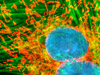
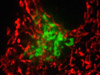
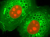
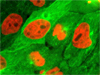
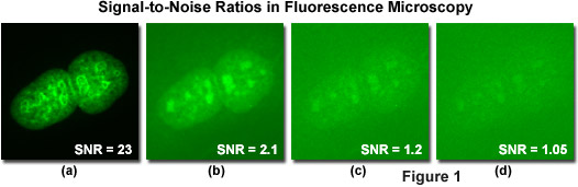
The effects of decreasing signal-to-noise ratio in fluorescence microscopy is illustrated by the series of digital images presented in Figure 1. The specimen is an adherent culture of opossum kidney proximal tubule epithelial cells (OK cell line) stained with SYTOX Green to image the nuclei. At high signal-to-noise ratios, a pair of interphase nuclei (Figure 1(a)) is imaged with sharp contrast and good definition of fine detail on a black background. As the signal-to-noise ratio decreases (Figures 1(b) and 1(c)), the definition and contrast of the nuclei also decrease until they almost completely blend into the noisy background (Figure 1(d)) as the SNR approaches unity.
During image acquisition with electronic sensors, including CCDs, noise superimposed on the signal is manifested as apparently random fluctuations in signal intensity, and as the magnitude of noise increases, uncertainty in the measured signal becomes greater (as illustrated in Figure 1). Signal-to noise ratio is typically evaluated in terms of the broad noise categories stated above, although each category may encompass several contributing noise components (discussed in following sections). The relative significance of each potential source depends upon the specific device and the type of application in which it is utilized. As stated, a large signal-to-noise ratio is important in the acquisition of high-quality digital images, and is particularly critical in applications requiring precise light measurements. Changes made to the factors that directly affect signal level, and to those variables primarily contributing noise to the system, obviously have an inverse effect on signal-to-noise ratio.
The measured signal from a CCD imaging system, utilized in calculating the signal-to-noise ratio, depends upon the photon flux incident on the CCD photodiodes (expressed as photons per pixel per second), the quantum efficiency of the device (where 1 represents 100 percent efficiency), and the integration time (exposure time) over which the signal is collected. The product of these three variables determines the signal portion (numerator) of the signal-to-noise ratio value, which is weighed against all noise sources that contribute to the denominator term of the ratio, and which degrade the performance of a CCD imaging device. Three primary undesirable signal components (noise) are typically considered in calculating overall signal-to-noise ratios:
Photon noise results from the inherent statistical variation in the arrival rate of photons incident on the CCD. Photoelectrons generated within the semiconductor device constitute the signal, the magnitude of which fluctuates randomly with photon incidence at each measuring location (pixel) on the CCD. The interval between photon arrivals is governed by Poisson statistics, and therefore, the photon noise is equivalent to the square-root of the signal. In general, the term shot noise is applied to any noise component reflecting a similar statistical variation, or uncertainty, in measurements of the number of photons collected during a given time interval, and some references use that term in place of photon noise in discussions of CCD noise sources.
Dark noise arises from statistical variation in the number of electrons thermally generated within the silicon structure of the CCD, which is independent of photon-induced signal, but highly dependent on device temperature. The generation rate of thermal electrons at a given CCD temperature is referred to as dark current. In similarity to photon noise, dark noise follows a Poisson relationship to dark current, and is equivalent to the square-root of the number of thermal electrons generated within the image exposure time. Cooling the CCD reduces the dark current dramatically, and in practice, high-performance cameras are usually cooled to a temperature at which dark current is negligible over a typical exposure interval.
Read noise is a combination of system noise components inherent to the process of converting CCD charge carriers into a voltage signal for quantification, and the subsequent processing and analog-to-digital (A/D) conversion. The major contribution to read noise usually originates with the on-chip preamplifier, and this noise is added uniformly to every image pixel. Certain types of noise in the CCD's output amplifier are frequency dependent (and consequently the application for which the camera is intended) and the required read-out rate or frame rate partially determine the read noise specification and its practical effect on overall signal-to-noise level. High-performance camera systems utilize design enhancements that dramatically reduce the significance of read noise.
The following equation is commonly used to calculate CCD camera system signal-to-noise ratio:
SNR = PQet /  PQet + Dt + Nr2
where P is the incident photon flux (photons/pixel/second), Q(e) represents the CCD quantum efficiency, t is the integration time (seconds), D is the dark current value (electrons/pixel/second), and N(r) represents read noise (electrons rms/pixel).
Careful examination indicates that the equation above is simply structured as a ratio of total signal generated during the exposure time divided by the combined noise attributable to the three primary noise components. The noise terms are not correlated, and the denominator incorporates appropriate values for each noise component: the square-root of the signal accounts for the photon noise, dark noise is equivalent to the square-root of the product of dark current and integration time, and the square-root of N(r)-squared corresponds to the read noise component.
The calculation of signal-to-noise ratios using the previous equation assumes that the signal is the only source of light. In the optical microscope, various sources of unwanted background light, such as scatter and reflections in the imaging system, may contribute noise, and if significant, this background photon flux (B) must be added to the photon noise component as follows:
SNR = PQet / (P + B)Qet + Dt + Nr2
An additional factor to be considered is that the values of incident and background photon flux, as well as quantum efficiency, are functions of wavelength, and when broadband illumination sources are employed, the calculation of signal-to-noise ratio requires these variables to be integrated over all wavelengths utilized for imaging.
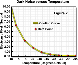
Various approaches are used to increase signal-to-noise ratio in high-performance CCD imaging systems. To reduce thermal charge generation within the semiconductor layers of the CCD, which is manifested as dark current, special device fabrication techniques and operation modes are sometimes employed. It is common to cool the CCD to reduce dark current to a negligible level using thermoelectric or cryogenic refrigeration, or if necessary, the extreme approach of liquid nitrogen cooling may be taken. In general, high-performance CCD sensors exhibit a one-half reduction in dark current for every 5 to 9 degrees Celsius as they are cooled below room temperature, a specification referred to as the doubling temperature. This rate of improvement typically continues to a temperature of approximately 5 to 10 degrees below zero, beyond which the reduction in dark current diminishes quickly (see Figure 2). In addition to specialized circuit and electronics design, filtration techniques utilizing advanced integrators and double sampling methods are sometimes undertaken to remove certain components of read noise.
Several manufacturers of high-performance CCD cameras provide a specification for "signal to noise" or "SNR", often expressed in decibels (dB). This value is equivalent to the ratio of the sensor's maximum pixel well capacity divided by the number of noise electrons resulting from on-chip thermal and electrical sources, neglecting photon noise, and should not be confused with the signal-to-noise ratio calculation described previously. It does not represent a determination of signal-to-noise ratio under specific operating conditions, but is a useful representation of a camera's dynamic range that is independent of how the camera is used. Under low-signal conditions, where read noise is the dominant noise source, the full SNR equation stated previously can be reduced to a simple ratio equal to the total signal collected during the integration time divided by the read noise value, a similar form to the dynamic range ("SNR") specification referred to here. The dynamic range value, however, corresponds to the limiting situation in which the full well capacity of a sensor element is reached, and is defined as follows:
Dynamic Range = Full Well Capacity (electrons) / Read Noise (electrons)
The full well capacity of a CCD represents the maximum charge (number of electrons) that can be stored in each pixel, and therefore determines the maximum signal available for a single read-out event. The ratio of the full well value (sometimes referred to as well depth or linear full well) to the number of per-pixel read noise electrons characterizes the ability of the device to capture both low and high signal levels in one image.
The dynamic range of a CCD and the true maximum bit depth of the camera's analog-to-digital converter are closely interrelated in that the total available signal relative to noise governs the maximum number of gray-level steps into which the signal can be divided. In order to represent subtle intensity differences in a digital image, it is necessary to discriminate as many gray-level steps as possible, and therefore a typical approach is to match analog-to-digital conversion bit depth to CCD dynamic range. The dynamic range relative to bit depth determines the number of electrons that comprise each gray level in the final image. Note that an analog-to-digital converter with a bit depth specification that exceeds the dynamic range of the CCD image sensor cannot attain its full theoretical range of grayscale discrimination (bit depth) because each gray-level step must correspond to a minimum difference of one signal electron.
As an example of appropriate strategy, a CCD with a full well capacity of 18000 electrons, and a read noise of 4 electrons per pixel at the specified read-out rate, has a dynamic range of 18000/4, or 4500. In order to utilize the full dynamic range of the CCD, a camera incorporating 12-bit analog-to-digital conversion is required, having the ability to detect 4096 (2 to the 12th power) grayscale levels (or 1.1 electrons per gray-level step). If 10-bit A/D conversion is used, only 1024 (2 to the 10th power) gray levels can be displayed, corresponding to 4.4 electrons per grayscale step. On the other hand, a camera having 14-bit A/D conversion, which has the capability of discriminating 16,384 gray levels, will be limited by the dynamic range (4500 electrons per pixel) of the CCD, and will not attain a satisfactory performance level.
A primary goal in the manufacture of scientific-grade CCD cameras is to maximize the signal available and minimize the noise, resulting in maximum dynamic range. By cooling the CCD to minimize thermal noise, as well as optimizing clocking, sampling, and other read-out electronics, the noise associated with each read-out cycle has been reduced in some high-performance cameras to as little as 3-5 electrons per pixel at typical read-out rates of approximately 1 megahertz. With the read noise of current CCDs nearing a likely lower limit, the remaining practical mechanism for improving dynamic range is to increase the available signal level. Although this can be accomplished by a CCD design incorporating larger pixels with very large full well capacity, there is an accompanying trade-off of lower spatial resolution in exchange for the improved effective sensitivity.
As previously discussed, the general category referred to as read noise actually comprises many sources, and dark current has not only an average component, but also exhibits a statistical fluctuation that contributes to shot noise. Although noise originates from different sources, its effect, in every instance, is to produce variations in image intensity. The level of detail required in modeling CCD noise depends upon the application, and generalizations adequate for evaluating the performance of camera systems are common. It is useful to describe, and to have an awareness of, most of the noise sources even though many may be reduced in practice to negligible levels. For signal-to-noise analysis, it is sometimes sufficient to consider only the on-chip amplifier noise, and most manufacturers provide this specification, referring to it as read noise, noise equivalent electrons, or the noise floor.
While read noise can be considered a noise floor with regard to electronics sources, under typical illumination conditions, the photon shot noise constitutes a natural fundamental limit on noise performance of a CCD camera (or any light detection system). Uncertainty in the number of photons collected during a specific time period is governed by Poisson statistics, and therefore the photon shot noise can be expressed as follows, in terms of equivalent electrons at the detector output:
Ns = S
where N(s) is the shot noise and S is the signal. With a detected signal of 2500 electrons, for example, the signal-to-noise ratio cannot exceed 2500/50, or 50, even with an ideal CCD, which contributes no noise due to dark current or signal read-out processes.
Due to the fact that photon noise is an inherent property of CCD signal detection, which cannot be reduced by camera design factors, it essentially represents the minimum noise level achievable for a system in which read noise and dark current noise are reduced to their minimum levels. Because of the square-root relationship of photon noise to signal, the noise level diminishes in relative magnitude as photon flux increases. Consequently, it is desirable to operate an imaging system under conditions that are limited by photon noise, with other noise components being reduced to relative insignificance. Under low light-level conditions (assuming dark noise is essentially eliminated by CCD cooling), read noise is greater than photon noise and the image signal is said to be read-noise limited. The camera exposure time (integration time) can be increased to collect more photons and increase the signal-to-noise ratio, until a point is reached at which photon noise exceeds both read noise and dark noise. At longer exposure times, the image is said to be photon-noise limited.
Within the broad categories considered above, a number of noise sources are always present even though they may be reduced or nearly eliminated, prior to final signal output, by system design or by careful operation within appropriate boundaries for a specific camera system. Photon shot noise and amplifier noise affect the amplitude of the detected signal, while other noise sources leave the amplitude unaffected, but produce fluctuations in the output value. Variations in image intensity resulting from noise accompanying the signal are reflected in the image display, both as pixel-to-pixel changes and differences in the same pixel from frame to frame. In addition, quantitative imaging techniques that rely on accurate pixel intensity measurements are affected by any variations attributable to noise. A number of additional noise sources that contribute to overall CCD performance are briefly described below.
Reset noise is induced when the charge collected in each pixel of a sensor array is converted (for measurement) from the charge domain to the voltage domain by employing a sense capacitor and source-follower amplifier. Prior to the measurement of each pixel's charge packet, the CCD sense capacitor is reset to a reference level. Noise is generated at the sense node by an uncertainty in the reference voltage level due to thermal variations in the channel resistance of the reset transistor (a metal oxide semiconductor field effect transistor; MOSFET). The reference level of the sense capacitor is therefore different from pixel to pixel, and the resulting noise is calculated as follows:
Nreset = 4kTBR
where N(reset) is the noise voltage on the sense node, k is Boltzmann's constant (joules/kelvin), T is temperature (kelvin), B refers to the noise power bandwidth (hertz), and R is the effective channel resistance (ohms). Reset noise can also be expressed in the customary units of equivalent electrons at the detector output, by restructuring the expression and introducing the fundamental value for electron charge, q (coulombs):
Nreset (rms electrons) = kTC / q
in which the additional symbol C represents the sense node capacitance (farads). This form of the equation is the origin of the commonly used term kTC noise as a synonym for reset noise.
Because reset noise can be significant (perhaps 50 rms electrons), most high-performance CCD cameras incorporate some mechanism to eliminate it. A common technique is to utilize a process referred to as correlated double sampling, in which a circuit measures the difference between the reset voltage and the signal voltage for each pixel, and assigns the resulting value of charge to the pixel. The additional step of measuring the output node reference voltage before each pixel charge is transferred makes it unnecessary to reset to the same level for each pixel. Other electronic methods are also available for eliminating reset noise, and are implemented according to the overall system design.
The read noise of a charge-coupled device arises from two primary noise components in the output amplifier, white noise and flicker noise. In similarity to the reset transistor, the output amplifier MOSFET has a resistance that generates thermal noise whose value is governed by the Johnson white noise equation. It is therefore either referred to as Johnson noise or simply as white noise, since its magnitude is independent of frequency. If the effective resistance is considered to be the output impedance of the source-follower amplifier, the white noise, in volts, is determined by the following equation:
Nwhite (volts) = 4kTBRout
where k is Boltzmann's constant (joules/kelvin), T is temperature (kelvin), B refers to the noise power bandwidth (hertz), and R is the output impedance of the amplifier (ohms). The white noise in terms of electrons at the CCD sense node is equivalent to the white noise in volts, defined above, divided by the product of amplifier sensitivity and output gain, as follows:
Nwhite (rms electrons) = 4kTBRout / Samp × Aamp
In the above equation, S is the amplifier sensitivity and A represents the amplifier gain. The sensitivity value is a function of the fundamental electron charge and the CCD sense capacitance and is expressed in units of volts per electron. Amplifier gain is simply a multiplication factor relating input volts to output volts (volt/volt).
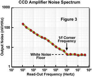
The second noise source attributed to the output amplifier is flicker noise, commonly referred to as 1/f noise because of its approximate inverse dependence on frequency. Many systems, both natural and manufactured, exhibit some form of 1/f behavior. With regard to CCD flicker noise, the significant frequency variable is the pixel read-out rate. For cameras in which pixels are read out at less than approximately 1 megahertz, and with a characteristic 1/f noise spectrum, the read noise floor is usually determined by 1/f noise. Figure 3 illustrates a typical CCD amplifier noise spectrum, plotting output noise as a function of read-out frequency. The reduction in noise as frequency increases is characteristic of a 1/f noise spectrum, exhibiting a decrease in noise by a factor of 3.16 for each decade increase in frequency. Note that the noise continues to decrease at this rate until it levels off, at a frequency referred to as the 1/f corner frequency. The stabilization of the noise level at higher frequencies indicates that the amplifier's white noise floor has been reached, and a pixel read-out rate greater than the 1/f corner frequency results in white noise limited operation. For the MOSFET amplifier producing the curve illustrated in Figure 3, the white noise floor occurs at approximately 4.5 nanovolts per root-hertz.
Flicker noise is generally accepted to originate due to the existence of interface states in the image sensor silicon that turn on and off randomly according to different time constants. All systems exhibiting 1/f behavior have a similar collection of randomly-switching states. In the MOSFET, the states are traps at the silicon-oxide interface, which arise because of disruptions in the silicon lattice at the surface. When electrons become trapped in the surface states, current flow is affected as the trapped electrons are released over a wide range of emission times governed by the various trap time constants. The silicon lattice disruptions that lead to the interface traps result in a distribution of energy levels of the traps within the forbidden gap. The range of trap depths at the silicon-silicon dioxide interface, and their varying time constants, determine the trap cutoff frequencies and produce a uniform distribution in energy throughout the silicon bandgap. The characteristic frequency distribution of the 1/f noise spectrum occurs because larger fluctuations are possible in the long time constant states (low frequencies), producing greater output fluctuations (noise), than are possible in the shorter time constant traps (high frequencies). Several different approaches are utilized in processing CCDs to reduce the density of these interface states, and in addition, silicon wafers having certain crystallographic orientations have lower inherent densities, making them preferred for CCD fabrication.
Dark current generation was previously discussed as a source of noise in CCD cameras, and it too is the result of lattice imperfections or impurities that introduce energy levels within the forbidden bandgap. Dark current is intrinsic to semiconductors and naturally results when electrons utilize thermal energy to move to intermediate steps in transition between the valence and conduction bands, allowing them to reach the conduction band where they are measured as signal. This current source is referred to as dark current because it continues to be produced when the CCD is in complete darkness. The rate of dark current accumulation in a pixel's potential well limits the integration time over which useful signal can be collected. Due to being thermally energized, dark current is most effectively reduced by cooling the CCD.
A number of specific regions in a CCD sensor contribute to dark current generation, including areas of neutral bulk silicon outside the potential well of a pixel, depleted material within the potential well, and surface states formed at the silicon-silicon oxide interface. In terms of the dark current level generated within each region of the CCD, the primary contributors are bulk dark current from the depleted region and surface dark current, with surface states being by far the dominant source. Bulk dark current in the absence of surface generation can be held to extremely low levels. The number of surface states can be reduced during manufacture by thermal treatment and passivation with various materials to minimize the number of broken or dangling bonds caused by the lattice mismatch at the epitaxial interface. Nevertheless, current generation centers at the silicon-silicon dioxide interface are typically 100 times more numerous than those in the bulk material.
Surface dark current varies greatly among different CCD manufacturers, depending upon the processing technology used in growth of the oxide layer and the passivation, along with other steps employed after oxide formation. Regardless of the techniques used to minimize formation of surface states, they remain the primary source of dark current. Although surface generation centers cannot be completely eliminated, their dark current contribution is greatly reduced by operation of the CCD in what is called inverted mode. CCDs that employ multi-pinned phase (MPP) technology operate in inverted mode, with greatly reduced dark current, leading to additional related advantages such as reduced cooling requirements.
Dark current generation at the silicon-oxide interface depends upon both the density of surface states and the density of free carriers (holes and electrons) at the interface. The presence of free carriers can fill the interface states and minimize the opportunities for electrons to thermally "hop" from interface states into the conduction band, essentially reducing dark current to the bulk current level. Operation of the CCD in normal (noninverted) mode results in maximum dark current generation because the interface and the signal channel are completely depleted of free carriers. Under inverted conditions, as employed with multi-pinned phase sensors, the CCD's array clock bias is changed to a negative state, inverting the signal carrying channel and causing minority carriers (holes) to migrate and populate the silicon-silicon dioxide interface. In this clocking scheme, also termed accumulation mode clocking, the holes in the inversion layer formed between the surface and the pixel well combine with electrons emitted from surface states, preventing them from being collected by the well as dark current. Inverted state operation has a significant effect on many CCD performance parameters in addition to the virtual elimination of surface dark current.
As stated, bulk dark current can be held to very low levels, and most of that collected by the pixel wells is generated within or near the depleted region of the pixels. The level of bulk dark current varies considerably among CCD manufacturers, and depends upon the quality of the silicon wafer material and the processing techniques employed prior to device fabrication. The mean dark current level originating in the bulk is related primarily to defects in the silicon, and various processing techniques, including gettering, are employed to remove impurities in regions of the sensor from which signal is produced. After device fabrication, the only mechanism for reducing bulk dark current is cooling the CCD. Dark current spikes are manifestations of unusually high dark current produced from a single pixel and are thought to result from silicon lattice imperfections or impurities. However, spikes do not necessarily follow the typical temperature behavior of other forms of dark current.
An empirical formula, or dark current equation, has been developed to describe the relationship between temperature and dark current produced by a CCD sensor. It precisely corresponds to dark current measurements taken in practice, and is valuable for determining the required operating temperature for elimination of camera dark current. The equation was developed from a general dark current formula, which is combined with an expression describing the variation of the bandgap energy of silicon with temperature, and a measured value of dark current at a standard temperature (300 K). The bandgap of silicon, E(g) (electron volts), varies with temperature according to the following, in which T represents temperature (kelvins):
Eg = 1.1557 - [(7.021 × 10⁻⁴ × T2) / (1108 + T)]
The resulting dark current formula is as follows:
D = 2.5 × 10¹⁵ × A × Id × T1.5 × e-Eg / (2kT)
in which D is the dark current (electrons/pixel/second), A is the pixel area (measured in square centimeters), I(d) is the dark current measured at 300 K (nanoamperes/square centimeter), T is the temperature (K), and E(g) is the bandgap at temperature T (electron-volts).
The noise associated with dark current is of two types, dark current shot noise and dark current non-uniformity. The shot noise component is governed by Poisson statistics, similarly to photon shot noise, and is equivalent to the square root of the dark signal. The only mechanism for reducing or eliminating dark current shot noise is cooling the CCD. Dark current non-uniformity is the variation of dark current from pixel to pixel in a sensor array, due to the fact that the pixels intrinsically have slightly different dark signal generation rates. This type of spatial noise is reduced by cooling, and is also subject to removal by image processing techniques, in which a dark reference frame is subtracted from each image. The reference frame is acquired under identical conditions of temperature and integration time as the image, but with the CCD blocked from all light.
An additional factor that produces non-uniformity in pixel output, and results in noise superimposed on the captured image, is photo response non-uniformity (sometimes abbreviated as PRNU). Due to variations in the array fabrication process, not all pixels exhibit the same sensitivity to light and an image of a uniformly illuminated flat-field will reflect a faint checkerboard pattern at the individual pixel level. The image processing technique of flat-fielding can be utilized to remove the pattern caused by the sensitivity variation. This involves subtraction of a separately acquired flat-field image from the specimen image data, which corrects for the non-uniformity in pixel sensitivity, although shot noise is increased by a factor of 1.414. Typically the non-uniformity is on the order 1-2 percent of the average signal level across the sensor array, and the significance of this noise component and the benefit in removing it depends upon the application.
Processing of the accumulated signal and its transfer to the output of a CCD sensor requires a number of clocking circuits, under control of a master clock. Clocking noise (or clock-jitter noise) can result from operation of these circuits if there is clock signal feed-through to the output waveform. The level of clock noise increases with signal and follows a square-root relationship to clocking frequency. Camera systems whose master clock is driven from a crystal oscillator do not usually exhibit problematic clock-jitter noise, but sensitivity improvements in sensors has increased the likelihood of clock signal feed-through occurring.
The limited number of photons available for image formation is a critical factor in many fluorescence microscopy techniques, and high-performance CCD camera systems are specifically designed to reach a photon-noise-limited operation mode at much lower signal levels than conventional cameras, which typically never achieve photon-noise-limited performance (and a suitably high SNR) at low light levels. In widefield microscopes, which commonly employ CCD cameras, the total signal available from the specimen focal volume may vary by several orders of magnitude, depending largely upon the imaging technique employed and the specimen itself. A photon flux of 10×(E6) (1 million) photons per second from the focal volume, an extremely low light level, is equivalent to an average of 1 photon/pixel/second distributed over the surface of a sensor having 1 million active pixels. As a point of reference, the minimum detection limit of the dark-adapted eye is approximately 40 times that (40 million photons/second). A properly designed fluorescence microscope typically yields 10×(E8) to 10×(E9) photons per second from the focal volume, or 100 to 1000 photons/pixel/second with the same 1-megapixel sensor. Conventional brightfield imaging mode commonly produces illumination levels, averaged over the full sensor area, of 5000 to approximately 40,000 photons/pixel/second. Unless the integration interval is very short, bright areas of a widefield image can generate a total detected signal of more than 100,000 photons per pixel.
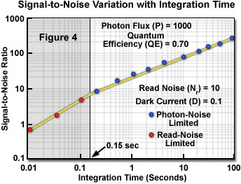
Figure 4 presents a plot of signal-to-noise ratio versus integration (exposure) time in a typical high-performance CCD camera designed for imaging at low signal levels, with photon flux and sensor characteristics fixed at the values shown in the figure. In a plot of this type, a read-noise-limited region and a photon-noise-limited region can be readily identified, separated at the exposure time for which photon noise begins to exceed read noise (approximately 0.15 second for the sensor and light flux values specified in the figure). Because of the square-root relationship of photon noise to signal, this division between the two regions occurs at an exposure time for which the total detected signal per pixel is approximately the square of the read noise value. For example, with a read noise specification of 5 electrons rms per pixel, photon noise becomes the dominant noise source when the exposure time is sufficient to result in more than 25 detected photons per pixel at the existing incident photon flux. The transition between the two dominant-noise regimes assumes that dark noise is negligible, which is typical in operation of scientific-grade CCD imaging systems, although other situations are possible. Operation at high dark-current levels alters the significance of the relative values of read noise and photon noise under some conditions, and in such circumstances dark noise can overwhelm both signal and other noise components.
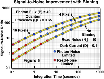
Many scientific-grade CCD cameras allow implementing an on-chip pixel binning function as another mechanism for increasing signal-to-noise ratio. It should be realized that this technique involves a sacrifice of some spatial resolution, as well as a concomitant increase in dark current. By improving the signal-to-noise ratio of the CCD, the imaging system is able to reach photon-noise-limited conditions at a lower light level and/or shorter exposure time. Some camera systems automatically utilize a pixel-binning mode for monitor display of a preview image to provide a brighter image at rapid frame rates, which facilitates specimen positioning and focusing. Figure 5 illustrates the effect of different binning values on curves plotting the variation of SNR with exposure time. The equation used for calculating SNR is modified to account for binning, as shown below:
SNR = MPQet / MPQet + MDt + Nr2
In this modified equation, the symbol M represents the number of binned pixels, and it is assumed that the signal in each of those pixels is the same. The three curves are plotted for the same typical CCD specifications, as denoted on the graph, and for a very low specimen signal intensity, producing a photon flux of 40 photons per pixel per second incident on the sensor. Note that without pixel binning, an exposure time of approximately 4 seconds is required to achieve a photon-noise-limited signal level. By implementing 16-pixel binning, an equivalent SNR and total number of detected photons per pixel is reached at an exposure time of only 0.25 seconds (see Figure 4), which would allow refreshing a preview image at an adequate frame rate to permit focusing and specimen positioning even at a low image intensity. Another consideration is that an image acquired using a 4-second integration time would benefit from an approximate 5-fold improvement in signal-to-noise ratio with the use of 16-pixel binning, compared to the unbinned mode. In many situations, particularly at low light levels, the benefits of reduced noise and the resulting improved image contrast outweigh the loss of theoretical spatial resolution that is inherent to the pixel binning process.
In practice, the microscopy technique chosen, in conjunction with the instrument and camera system being used, determine the values of most parameters that are relevant to the signal-to-noise ratio achieved. The photon flux is usually a function of the illumination system and imaging mode employed, while the CCD characteristics are determined by design and manufacturing factors and generally cannot be improved later (assuming that cooling is provided as required). Consequently, the microscopist typically has only the control of integration time, and perhaps implementation of on-chip binning, as mechanisms for increasing the detected signal and signal-to-noise ratio.
Contributing Authors
Thomas J. Fellers and Michael W. Davidson - National High Magnetic Field Laboratory, 1800 East Paul Dirac Dr., The Florida State University, Tallahassee, Florida, 32310.