
Image Galleries
Featured Article
 Electron Multiplying Charge-Coupled Devices (EMCCDs)
By incorporating on-chip multiplication gain, the electron multiplying CCD achieves, in an all solid-state sensor, the single-photon detection sensitivity typical of intensified or electron-bombarded CCDs at much lower cost and without compromising the quantum efficiency and resolution characteristics of the conventional CCD structure.
Product Information
Review Articles
Concepts in Digital Imaging Technology
Electron Multiplying Charge-Coupled Devices (EMCCDs)
The inherent advantages of scientific charge-coupled device (CCD) sensors for digital imaging in optical microscopy have made them ubiquitous in a wide variety of applications. One of the few significant shortcomings of conventional high-performance CCD cameras is that very low signal levels typically fall beneath the read noise floor of the sensor, limiting the imaging capabilities in a number of currently productive research areas that demand rapid frame-rate capture at extremely low light levels. An innovative method of amplifying low-light-level signals above the CCD read noise is employed in electron multiplying CCD technology. By incorporating on-chip multiplication gain (see Figure 1), the EMCCD achieves, in an all solid-state sensor, the single-photon detection sensitivity typical of intensified or electron-bombarded CCDs at much lower cost and without compromising the quantum efficiency and resolution characteristics of the conventional CCD structure.
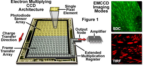
The primary feature that distinguishes this novel new technology is the inclusion of a specialized extended serial register on the CCD chip that produces multiplication gain through the process of impact ionization in silicon. By elevating photon-generated charge above the read noise of the device, even at high frame rates, the EMCCD has the capability of meeting the needs of ultra-low-light imaging applications without the use of external image intensifiers. Consequently, the approach is applicable to any of the current CCD sensor architectures, including back-illuminated devices, and sensors employing electron multiplying registers are considerably less expensive to manufacture due to the signal amplification stage being incorporated directly into the CCD structure.
Several major areas of current research focus in the biomedical sciences rely on specific targeting of subcellular structures or single molecules with appropriate fluorophores in order to follow the dynamics of biological processes. The rapid kinetics combined with extremely small specimen volumes and low fluorophore concentrations utilized in such experiments require both high sensitivity and rapid frame-rate data acquisition. In the evaluation of transient, low-intensity signals, such as those encountered in single-molecule investigations, total internal reflection fluorescence (TIRFM; see Figure 1), spinning disk confocal in live-cell imaging, flux determinations of calcium or other ions, and time-resolved three-dimensional microscopy (4-D techniques), the electron multiplying CCD offers significant advantages over other sensors designed for low signal levels. Additionally, when employed with the higher signal levels of conventional fluorescence imaging techniques, the extreme sensitivity of the EMCCD system allows the use of lower fluorophore concentrations and/or lower power levels from the excitation source, thereby reducing both the potential toxicity to living cells and photobleaching of the fluorescent probe.
The performance of all CCD-based detectors has improved dramatically in recent years, and increased sensitivity has lowered detection limits in high-performance low-light imaging systems significantly. Quantum efficiency now exceeds 90 percent and read noise is limited to less than 4 electrons rms (root-mean-square) in some high performance back-illuminated CCD camera systems. This low level of read noise performance is attainable in traditional CCD sensors only at moderate readout rates, however. In addition, because the charge packet from a single pixel is often only a few electrons in challenging microscopy investigations, the signal is too frequently lost in the read noise even at slow readout rates. Furthermore, when imaging is performed at video frame rates and faster, the read noise increases to an unacceptable level, relative to the signal, in low-light conditions.
One proven solution to the read noise limitation when higher frame rates are required has traditionally been to employ an image intensifier to multiply the number of emitted specimen photons prior to detection and readout by a conventional CCD. In this approach, which is based on an operation principle similar to that of photomultiplier tubes, the signal is amplified to a level that exceeds the read noise generated at the desired frame rate. The intensified CCD (ICCD) camera system is presently among the most commonly employed imaging methods for low-light techniques such as time-resolved fluorescence experiments, ratio imaging of ion-sensitive fluorochromes, single molecule fluorescence, and other dynamic studies in living cells. These systems are sometimes referred to as proximity-focused image intensifiers and utilize a photocathode closely coupled to a micro-channel plate (MCP) electron multiplier.
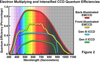
The amplified electron output from the MCP is accelerated by a high potential difference onto a phosphorescent screen that converts the electrons to photons, which are subsequently relayed to the CCD surface through an optical relay lens or direct fiber optic coupling. Because potential differences ranging from 2500-5000 volts are maintained to accelerate electrons across the gaps separating the components of the ICCD, a high internal vacuum is necessary, requiring the device to be precisely assembled and completely free of contaminants. The manufacturing costs are consequently relatively high, and the intensifiers present certain other disadvantages as well, among them reduced spatial resolution compared to an equivalent conventional (non-intensified) CCD, high background noise, relatively low quantum efficiency (Figure 2), and susceptibility to irreversible damage from exposure to high light levels.
The resolution of the ICCD is ultimately limited by the resolution of the photocathode, the micro-channel plate, and the output phosphor. Continued improvements in the phosphor composition and microchannel plate architecture of modern devices has resulted in resolutions of 64 line pairs per millimeter, or better, which corresponds to a full-width at half maximum (FWHM) spot size of approximately 25 micrometers. Unfortunately, for single electron recording events (necessary in single molecule imaging) about 50 percent of the signal is spread into neighboring pixels with an ICCD, which results in considerable spatial averaging compared to an EMCCD. This effect must be carefully scrutinized when examining data collected during single molecule experiments using ICCD detector systems.
Electron-bombarded CCDs (EBCCD) are a less widely used detector variation for low-light camera systems, and in similarity to intensified CCDs, incorporate a photocathode for photon-to-electron conversion, followed by acceleration across a high-voltage gradient. The energetic electrons impinge directly on a back-thinned CCD, where they generate multiple charges, resulting in a modest signal gain. The devices can be operated at video frame rates, but have limited gain adjustment range, and exhibit similar disadvantages to the intensified CCD, including reduced quantum efficiency and resolution, and the potential for damage to the external image-intensifying components if exposed to high light levels. The development of the electron multiplying CCD employing on-chip multiplication gain provides the basis for cameras that achieve the signal gain benefit of systems using external intensifiers, while maintaining the customary CCD advantages of high, spectrally broad quantum efficiency (Figure 2), full native pixel resolution, and immunity to damage from high light levels.
Diagrammed in Figure 2 are the quantum efficiencies and spectral profiles of front and back illuminated electron multiplying CCDs, as well as the photocathodes in popular Gen II and Gen III intensifiers. The back-thinned CCD has a quantum efficiency of 90-percent or greater over the wavelength region of 500 to 700 nanometers and exhibits the highest values of any device in the near-infrared. In contrast, the front-illuminated CCD features a much lower quantum efficiency (approximately 60 percent) over a narrower wavelength range of 550 to 700 nanometers. Both of the CCD devices depicted in Figure 2 have significantly greater quantum efficiencies than the Gen intensifiers, which range between 35 and 45 percent in the visible spectral region. Intensifier photocathodes designed to operate more efficiently in the ultraviolet and infrared region are available.
On-Chip Multiplication Gain
Conventional cooled CCD cameras achieve relatively high sensitivity through the process of integrating signal within each pixel prior to readout in order to overcome read noise, which is incurred only once for each frame. At low light levels, long exposures are required in order to accumulate sufficient signal and achieve the detector's maximum read-noise performance. Consequently, frame rate speeds are limited to a relatively slow fraction of a frame up to a few frames per second. In applications suitable for "slow-scan" signal acquisition, for which the detector can be operated in the photon shot noise-limited regime, traditional back-illuminated CCD systems provide superior overall performance, including maximum quantum efficiency (as illustrated in Figure 2), which takes into account noise factors associated with electron multiplication. However, when it is necessary to capture temporal data requiring video frame rates or faster, at very low light levels, the conventional CCD camera is fundamentally limited by read noise.
The electron multiplying CCD incorporates a structural enhancement to amplify the captured signal before the charge is transferred to the on-chip amplifier, which has the effect of reducing the read noise, relative to signal, by the value of the multiplication gain factor. Because very weak specimen signal levels may produce a charge packet from a single pixel of only a few electrons, even with slow readout from a high-performance CCD, the signal is lost in read noise. The primary advantage of the EMCCD is to provide a mechanism to improve signal-to-noise ratio for signal levels below the CCD read-noise floor. In applications that require extremely fast gating (on the nanosecond level), the EMCCD is not appropriate, and intensified CCDs maintain an advantage in rapid kinetic data collection of this type.
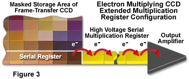
Electron multiplying CCD sensors are produced utilizing conventional CCD fabrication techniques by making relatively simple structural modifications. The unique feature of the EMCCD is an electron multiplying structure (in effect, a charge amplifier) positioned between the end of the shift register and the output node, which is often referred to as the multiplication register or gain register (see Figure 3). This special extended serial register provides multiplicative gain following detection of photons in the device's active pixel array, and therefore, the technology can be adapted to any current CCD architecture and format. The most widely used sensors produced by the two companies that pioneered the technology employ frame-transfer architecture, and camera manufacturers have also introduced systems based on back-illuminated versions of the electron multiplying CCDs.
The functional layout of a frame-transfer electron multiplying CCD is illustrated in Figure 3, in which the gain register is added to the charge transfer path following the frame-transfer area of the chip and the conventional serial register, and preceding the on-chip charge-to-voltage conversion circuitry. The structure of the additional register differs from the regular shift register in that the full-well capacity is increased and electrons are accelerated from element to element in the multiplication register by application of much higher clock voltages at selected transfer electrodes. When charge is transferred by applying a higher-than-normal voltage, secondary electrons are generated in the silicon by the process of impact ionization. In the gain multiplying register, each stage comprises four gates, three of which are clocked as in the conventional 3-phase structure, with the fourth (between phases 1 and 2) being held at a low fixed direct current (DC) potential.
Figure 4 illustrates the transfer of charge through the gates. Note that the gates for phases 1 and 3 (R1 and R3) are clocked with drive pulses of normal potential, which is typically on the order of 5 to 15 volts (the R3 gates have zero potential for the clocking phase illustrated in Figure 4). The clock pulses used in the same phases of the regular readout register can be employed for these gates. Phase 2 (R2 in Figure 3) is clocked at higher voltage (35-50 volts) preceded by a gate held at a low DC level (denoted by the Low DC gate in Figure 4). The potential difference between the fixed-level gate and the high-voltage clocked gate results in sufficient field intensity to sustain the impact ionization process as electrons are transferred from phase 1 to phase 2 in the normal clocking sequence. Although the charge multiplication per transfer is only on the order of 1.01 to 1.016, the gain accumulated over the large number of pixels in the multiplication register (dependent on the horizontal pixel array size) is substantial, and can be hundreds or thousands. The multiplication gain is exponentially proportional to the applied high phase-2 voltage, and can be increased or decreased by varying the clock voltages.
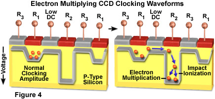
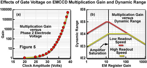
Figure 5(a) illustrates the exponential increase in gain that accompanies increasing amplitude of the clocking voltage applied to the phase 2 electrode. It is obvious that relatively small adjustments to the voltage, beyond a certain value, result in large changes in the on-chip multiplication gain. In commercial EMCCD camera systems, this voltage adjustment is commonly mapped to a high-resolution digital-to-analog converter that can be precisely controlled through computer software. In spite of the very low probability of impact ionization occurring and the low mean gain per stage, the overall gain factor in the multiplication register can easily be in excess of 1000x due to the large number of pixels over which the electron charge packet grows in cascading fashion. The probability of secondary electron generation is dependent on the serial clock voltage levels and the CCD temperature, and as indicated above, typically ranges from 1 to 1.6 percent. While the probability of secondary electron generation is described by a complex function, the total gain (M) of the cascaded elements in the multiplication register is given by the following equation:
M = (1 + g)N
where g is the probability of generating a secondary electron and N is the number of pixels in the multiplication register. A CCD having 512 elements in the gain register and an impact ionization probability of 1.3 percent (0.013) would, therefore, generate a total charge multiplication gain of over 744.
Because of the (exponential) relationship of the multiplication gain to clock voltage, a wide adjustment range is available, allowing setting the gain to a sufficiently high level to effectively reduce readout noise to insignificant levels under most imaging conditions. Since the multiplication gain is independent of readout speed, setting a gain level equivalent to the read noise in electrons, at the desired readout frequency, produces an effective noise level of 1 electron rms. Increasing gain beyond this range will reduce noise to sub-electron levels. Significantly, by utilizing higher gain settings at faster frame rates, this noise performance can be achieved at any speed. As an example, a current high-performance back-illuminated electron multiplying CCD, with a read noise specification of 60 electrons rms at 10 megahertz, can achieve a sub-electron effective noise level with any on-chip multiplication gain value of 60 or greater.
As discussed, electron multiplication gain can be used to overcome any readout noise, although it is desirable to minimize this factor because at some level, increasing gain results in a limitation of sensor dynamic range (as illustrated in Figure 5(b)). Although the bit depth of the analog-to-digital converter of the camera system determines the maximum dynamic range, at gain levels beyond that required to overcome read noise, dynamic range will decrease due to the multiplied signal exceeding the pixel full well capacity and/or the magnitude of the output amplifier. For example, if a register designed to contain a normal full-well charge of 200,000 photoelectrons is used at a gain level of 250x, then pixels at the end of the gain register will become saturated whenever the original charge packet is greater than 800 photoelectrons. By taking specific design steps to maximize full well depth and amplifier throughput, camera manufacturers are able to provide for high bit-depth imaging with moderate gain and at high frame rates. Because this requires the readout amplifier to be optimized for larger pixels at high speeds, the read noise specification is necessarily increased. In addition, the ultimate size of a register pixel is limited by the fact that a triplet of transfer electrodes can only control photoelectrons over a maximum silicon band size of approximately 18 micrometers.
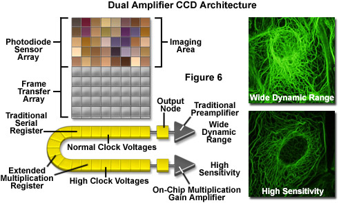
Increasing the EMCCD multiplication gain factor overcomes higher levels of read noise, but the dynamic range of the camera system suffers, limiting the use of the camera with brighter signals amenable to slower readout. To maintain full dynamic range, some electron multiplying camera systems are being equipped with dual amplifiers (see Figure 6), including a conventional unit for slow-scan wide dynamic range applications such as brightfield or fluorescence imaging, as well as a high-speed amplifier for high-sensitivity operation requiring the use of on-chip gain. Such a combination provides a camera system with the traditional CCD advantages of high resolution, high quantum efficiency, and wide dynamic range coupled to the highest sensitivity achievable.
Additional Noise and Performance Variables
Several additional factors are significant with regard to the performance of electron multiplying CCDs, including the relationship between on-chip gain and dynamic range (discussed above), other gain-related noise sources, evaluation of quantum efficiency, a phenomenon known as gain ageing, and considerations regarding cooling requirements of the image sensors. The efficiency of the impact ionization process, which produces charge gain during electron transfer in the specialized serial register, is inversely dependent on temperature. The probability of secondary electron generation increases as temperature is decreased, and consequently a camera equipped with a well designed cooling system is able to achieve higher gain values at lower clock voltage settings.
The optimum level of cooling depends on the camera system and application, but the variation of multiplication gain with temperature illustrates the importance of maintaining precise temperature stability in order to avoid adding noise to the measured signal. Dark noise arising from thermal dark current generation in the electron multiplying CCD is identical to that in conventional CCDs, and is similarly reduced by cooling the sensor. With conventional high-performance detectors, the sensor is usually cooled to a temperature at which dark current shot noise arising during the expected integration (exposure) interval is negligible. Once the dark noise is substantially lower than the noise associated with signal readout, further cooling does not provide any additional practical benefit.
Electron multiplying CCD cameras are able to detect even single-photon events when the on-chip multiplication is utilized to elevate the signal above the read noise level, and it must be recognized that any level of unsuppressed dark current is significant since it is subject to being multiplied along with the signal. Ideally, therefore, the dark current should be completely eliminated in the EMCCD, and cooling systems designed to reduce CCD temperature to -75 degrees Celsius or lower are incorporated in the most advanced camera systems.
Note that different noise components are relevant in intensified CCD systems. While signal is amplified above both dark current and read noise in the ICCD, making increased cooling less beneficial, another source of noise arising in the intensifier photocathode, referred to as equivalent background illuminance (EBI), occurs in intensified systems. The electron multiplying CCD does not exhibit EBI, and overall, dark current is a less significant limitation for the EMCCD with effective cooling than EBI is for intensified CCD cameras. Although increased cooling can reduce EBI in the photocathode, effective cooling systems for the more complicated multi-component structure of intensified CCDs, which usually include fiber optic couplings, are much less practical.
Due to the probabilistic nature of the impact ionization process utilized in the EMCCD, a statistical variation occurs in the on-chip multiplication gain. The uncertainty in the gain produced introduces an additional system noise component, which is evaluated quantitatively as the excess noise factor (or simply noise factor, abbreviated F), and which acts as a multiplying factor for both dark and photon-generated signal in the camera system. Excess noise factors vary for the different low-signal detector types, and are attributable to a combination of various loss mechanisms (if they exist) and to statistical variation in the electron multiplication process arising either in the silicon crystal lattice of the EMCCD or the micro-channel plate of the ICCD.
A conventional CCD that does not have any significant loss mechanisms or additional noise from amplification processes exhibits a noise factor of unity, as does an EMCCD utilizing normal clock voltages and producing no multiplication gain. With increased gain settings, the statistical variations begin to add additional noise, the magnitude of which depends upon both the gain and the signal level. According to theory, the excess noise factor for the electron multiplication process is approximately 1.4 (square root of 2) over a wide range of gain levels. Experimental measurements are typically lower, and range between 1.0 and 1.4 for multiplication gain factors up to 1000x. A value of 1.3 is a commonly stated average for EMCCDs, in comparison to noise factors of 1.6 to 2 for intensified CCDs employing Gen II and Gen III filmed and filmless photocathodes. Filmed image intensifiers generally have higher noise factors because of the additional loss mechanism imposed on electrons by the film.
One noise phenomenon that exists in the EMCCD, and which has no equivalent in intensified CCDs, is referred to as spurious charge or clocking induced charge (CIC). When electrons are being transferred through the multiplication register under the influence of clocking pulses, the sharp clock waveform inflections produce impact ionization in a small proportion of transfers even with normal clocking voltages. Furthermore, the clock pulses may produce a secondary electron even when no primary electron is present for transfer. By careful manipulation of clock waveform amplitudes and edges, manufacturers can minimize CIC, which is normally estimated to produce only one electron in approximately 100 transfers. Even in high-performance low noise conventional CCDs, clocking induced charge is totally lost in readout noise; however in the EMCCD at high gain settings, additional CIC is generated, and is generally treated as an additional component of dark-related signal.
Clocking induced charge is independent of exposure time, but because it is attributed to impact ionization, it is usually considered to increase with decreasing temperature, just as electron multiplication does. When EMCCDs are utilized at high gain, single electron events are recorded as spikes in the image, and any contribution from CIC would seemingly be visible. Under typical operating conditions of the EMCCD, background events causing such spikes, rather than readout noise, determine the detection limit of the camera. Recent dark image tests performed at various cooling temperatures by one manufacturer indicate that whatever the CIC contribution is to dark current, it does not appear to set a cooling limit as temperature is reduced to as low as -95 degrees Celsius. In those tests background spikes appearing above readout noise are attributed to dark current, and are dramatically reduced as temperature is lowered.
Evaluation of the signal-to-noise ratio (SNR) of an electron multiplying CCD requires that the conventional expression applied in the calculation for CCD sensors be modified to reflect the effect of on-chip multiplication gain and the excess noise factor. In effect the SNR is equivalent to the total number of photons detected per pixel during the integration interval divided by the combined noise from all sources, as follows:
SNR = (S × Qe) / Ntotal
where S represents the number of incident photons per pixel, and Q(e) is the quantum efficiency, or proportion of total photons actually detected as signal. The total noise in the system is represented by N(total), which combines several variables according to the following relationship:
Ntotal =  (S × Qe × F2) + (D × F2) + (Nr / M)2
where F represents the excess noise factor, D is the total dark signal, N(r) is the camera read noise, and M is the on-chip multiplication gain. The noise terms in the denominator of the EMCCD noise equation represent the familiar CCD noise components, photon shot noise, dark noise, and read noise, respectively, with appropriate modifications to account for loss mechanisms and statistical noise sources specific to the process of on-chip multiplication gain. This is accomplished by applying the excess noise factor (F) to the first two terms, and the multiplication gain factor (M) to the read noise term. The effective shot noise and dark noise are increased by the excess noise factor, while read noise is reduced by the multiplication gain achieved in the gain register.
Both electron multiplying and intensified CCDs suffer from a gain degradation artifact known as gain ageing, which occurs in the gain register or microchannel plate of the devices. In EMCCDs, gain ageing is manifested by a slow decrease in gain over time and is quantitatively based on the total electric charge that has passed through the multiplication register. Although the exact nature of gain ageing has not been fully elucidated, CCD designers speculate that the high voltages used in the multiplication process (30 to 50 volts) trap accelerated electrons in the silicon-silicon dioxide interface region beneath the transfer electrode. The trapped electrons effective alter the electric field gradient at this point and thus create the gain ageing phenomenon. Gain ageing occurs exponentially over time and is most prominent during the first hours of use in the EMCCD gain register.
In order to compensate for gain ageing, commercial camera manufacturers often pre-age cameras at high gain settings for several hundred hours or more before readjusting the circuitry. Additionally, several manufacturers are now using computer algorithms to compensate for gain ageing and protect the gain register. Gain ageing can be controlled by reducing the gain and blocking illumination when the camera is not being used. In general, the gain should be adjusted to a level that just offers sufficient gain to overcome the readout noise. No further increase in the signal-to-noise ratio is achieved once the readout noise becomes less than one, and continuing to add gain only enhances the rate of gain degradation. Finally, the investigator can periodically monitor gain characteristics with a standardized specimen to ensure maximum performance from EMCCD cameras.
The solid-state on-chip electron multiplication of the EMCCD gives it a number of decided advantages over intensified CCDs, including preservation of the spatial resolution of the CCD, and superior quantum efficiency performance due to not being constrained by limitations of the intensifier phosphor. In comparing quantum efficiencies of different detector types, the effect of all loss mechanisms and statistical noise sources must be considered. In terms of the resulting effective quantum efficiencies, electron multiplying CCDs, particularly back illuminated versions, exhibit substantially broader and higher quantum efficiency values than any other low-light detector.
Contributing Authors
Thomas J. Fellers and Michael W. Davidson - National High Magnetic Field Laboratory, 1800 East Paul Dirac Dr., The Florida State University, Tallahassee, Florida, 32310.