Image Galleries
Featured Article
 Electron Multiplying Charge-Coupled Devices (EMCCDs)
By incorporating on-chip multiplication gain, the electron multiplying CCD achieves, in an all solid-state sensor, the single-photon detection sensitivity typical of intensified or electron-bombarded CCDs at much lower cost and without compromising the quantum efficiency and resolution characteristics of the conventional CCD structure.
Product Information
Review Articles
Concepts in Digital Imaging Technology
Electronic Shutters
Electronic shutters are employed in charge-coupled devices (CCDs) to control integration time (exposure) of the photodiode array and reduce blooming, overexposure, and smear when capturing moving objects using time-lapse or full motion video in the microscope.

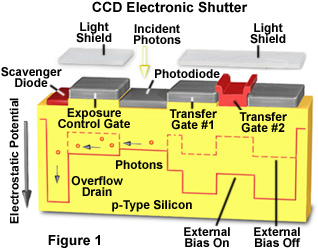
Presented in Figure 1 is a diagrammatic illustration of a CCD pixel that is equipped with an electronic shutter exposure control gate. The shutter is used to vary the integration time by draining all charge from a photodiode potential well for a fraction of the total integration time. Electronic shutters usually operate in stepped increments, decreasing the collected illumination (exposure time) by 50 percent for each step.
Integration of electrons in the photodiode potential well is controlled by the exposure control gate, which will shunt electrons to the scavenger diode when biased to the "on" state by the CCD clock circuitry. In some CCD configurations, the electronic shutter can be used to balance the color response of the red, green, and blue channels.
Shutters allow all light sensitive photodiodes to be simultaneously erased without affecting darkened shift registers, thus controlling the time period between flushing the photodiodes and the start of the readout process. The exposure rate of an electronic shutter can vary between 1/60th and 1/16,000 second, depending upon CCD architecture.
Contributing Authors
Mortimer Abramowitz - Olympus America, Inc., Two Corporate Center Drive., Melville, New York, 11747.
Michael W. Davidson - National High Magnetic Field Laboratory, 1800 East Paul Dirac Dr., The Florida State University, Tallahassee, Florida, 32310.


