
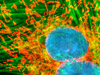
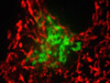
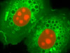
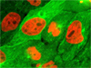
Image Galleries
Featured Article
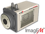 Electron Multiplying Charge-Coupled Devices (EMCCDs)
By incorporating on-chip multiplication gain, the electron multiplying CCD achieves, in an all solid-state sensor, the single-photon detection sensitivity typical of intensified or electron-bombarded CCDs at much lower cost and without compromising the quantum efficiency and resolution characteristics of the conventional CCD structure.
Product Information
Review Articles
Concepts in Digital Imaging Technology
Four Phase CCD Clocking
Charge transfer through CCD shift registers occurs after integration to relocate accumulated charge information to the sense amplifier, which is physically separated from the parallel pixel array. Several clocking schemes, including the four phase technique illustrated in Figure 1, are utilized to transfer charge from the collection gates to the output node.
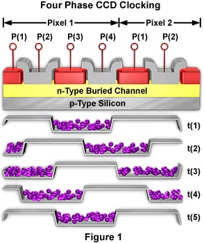
A four phase CCD incorporates four individual polysilicon gate electrodes in each pixel cell, each of which requires a separate input clock signal to properly transport accumulated charge. The shift register illustrated in Figure 1 includes one and a half pixel elements, for a total of six gates aligned along a common axis to form a column. The nature of electrostatic forces in the silicon substrate beneath the gates is determined by the voltage level applied to a particular gate by the clock input signal. High level voltages induce the formation of a potential "well" beneath the gate, whereas low level voltages form a potential barrier to electron movement.
Figure 1 illustrates a timing diagram utilizing a series of voltage schemes to transport charge through a four phase CCD. At t(1), the voltage applied to gates P(1) and P(2) is held low while that applied to gates P(3) and P(4) is held high. This causes the creation of a potential well, which is formed beneath gates P(3) and P(4) to integrate charge collected by Pixel 1 (illustrated as a collection of purple "electrons"). To transfer charge, at t(2) the voltage applied to gates P(1) and P(3) changes polarity with P(1) going from low to high and P(3) going from high to low. Electrostatic forces subsequently move the charge packet (purple electrons) a single step to the new potential well formed beneath gates P(4) of Pixel 1 and P(1) of Pixel 2. The net effect is to transfer the integrated charge one gate width to the right in figure 1. At clock interval t(3), gates P(2) on both pixels switch from low to high, while gate P(4) on Pixel 1 switches from high to low. This action forces the charge packet a single step further to a new potential well formed under gates P(1) and P(2) of Pixel 2. Simultaneously, another new potential well is created under gates P(1) and P(2) of Pixel 1 to accommodate transferred charge from Pixel 0 (not illustrated). A single cycle of the process is completed at t(4), when the charge is transferred to new potential wells created under gates P(2) and P(3) of both Pixels 1 and 2. The entire process is repeated until all charge packets have reached the output node. Note that even though only a single charge packet is being moved in Figure 1, this clocking scheme simultaneously transfers all charges associated with the columnar gate array.
The charge transfer process is termed readout, and is controlled by a series of clocks that operate on all gates in the array, including the transfer gate between serial and parallel registers and the photodiode reset gates. This cascade of clocking schemes is used to operate the CCD in a controlled and efficient manner.
Contributing Authors
Mortimer Abramowitz - Olympus America, Inc., Two Corporate Center Drive., Melville, New York, 11747.
Michael W. Davidson - National High Magnetic Field Laboratory, 1800 East Paul Dirac Dr., The Florida State University, Tallahassee, Florida, 32310.