Image Galleries
Featured Article
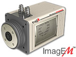
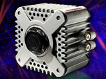
 Electron Multiplying Charge-Coupled Devices (EMCCDs)
By incorporating on-chip multiplication gain, the electron multiplying CCD achieves, in an all solid-state sensor, the single-photon detection sensitivity typical of intensified or electron-bombarded CCDs at much lower cost and without compromising the quantum efficiency and resolution characteristics of the conventional CCD structure.
Product Information
Interactive Flash Tutorials
CCD Clocking Schemes
Charge transfer through CCD shift registers occurs after integration to relocate accumulated charge information to the sense amplifier, which is physically separated from the parallel pixel array. This tutorial explores several clocking schemes that are utilized to transfer charge from the collection gates to the output node.
The applet initializes with a deactivated four-phase clocking scheme loaded into the window. Start the applet by selecting the Auto button, which will run the charge transfer automatically. Electrons comprising the integrated charge are represented by a green pool that is transferred through energy minima from one gate to the next. To step through the sequence manually, either click the Manual button to halt automatic transfer, or click on the Next >> button. Each click on the button will advance the tutorial a single step. Use the radio buttons to toggle between two-, three- and four-phase CCD clocking schemes.
The charge transfer process is termed readout, and is controlled by a series of clocks that operate on all gates in the array, including the transfer gate between serial and parallel registers and the photodiode reset gates. This cascade of clocking schemes is used to operate the CCD in a controlled and efficient manner.
Contributing Authors
Mortimer Abramowitz - Olympus America, Inc., Two Corporate Center Drive., Melville, New York, 11747.
Clay Krauterbluth and Michael W. Davidson - National High Magnetic Field Laboratory, 1800 East Paul Dirac Dr., The Florida State University, Tallahassee, Florida, 32310.


