Image Galleries
Featured Article
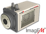
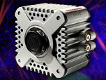
 Electron Multiplying Charge-Coupled Devices (EMCCDs)
By incorporating on-chip multiplication gain, the electron multiplying CCD achieves, in an all solid-state sensor, the single-photon detection sensitivity typical of intensified or electron-bombarded CCDs at much lower cost and without compromising the quantum efficiency and resolution characteristics of the conventional CCD structure.
Product Information
Interactive Flash Tutorials
CCD Operation
Explore the operation of a charge-coupled device (CCD) imaging semiconductor with this interactive Flash tutorial. Modern CCDs consist of a light-sensitive sandwich of insulating silicon dioxide positioned beneath an array of photodiodes and above an array of metal electrodes.
Photons from an illumination source (shown in the tutorial as a wavy red arrow) first collide with silicon atoms in the body of the CCD, releasing negatively charged electrons. These electrons are trapped in the pixel array with a positive charge generated by the electrode array positioned beneath an insulating layer of silicon dioxide. In this manner, light intensity from an object being imaged is captured in terms of the number of electrons contained in each pixel.
The second stage consists of reading the number of electrons stored in each pixel, one at a time, until the entire array has been translated to produce a video signal. This is accomplished by a ripple voltage that runs along the electrodes of each pixel column, dragging the electrons from one pixel to another. The electrons positioned in pixels adjacent to the horizontal readout register are transferred onto this row, then sequentially read in a serial manner until the contents of the entire CCD has been recorded. When all columns have emptied into the readout register and been converted into a continuous waveform, the process repeats itself.
Contributing Authors
Mortimer Abramowitz - Olympus America, Inc., Two Corporate Center Drive., Melville, New York, 11747.
Clay Krauterbluth and Michael W. Davidson - National High Magnetic Field Laboratory, 1800 East Paul Dirac Dr., The Florida State University, Tallahassee, Florida, 32310.


