Image Galleries
Featured Article
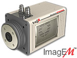
 Electron Multiplying Charge-Coupled Devices (EMCCDs)
By incorporating on-chip multiplication gain, the electron multiplying CCD achieves, in an all solid-state sensor, the single-photon detection sensitivity typical of intensified or electron-bombarded CCDs at much lower cost and without compromising the quantum efficiency and resolution characteristics of the conventional CCD structure.
Product Information
Interactive Flash Tutorials
CCD Electronic Shutters
Electronic shutters are employed in charge-coupled devices (CCDs) to control integration time (exposure) of the photodiode array and reduce smear when capturing moving objects in the microscope. Instructions for operation of the tutorial appear beneath the applet window.
The tutorial initializes with the bias turned off to both the shutter and transfer gates so that the photodiode can proceed with charge integration. Use the mouse cursor to activate the Exposure button and trigger a sequence of shutter drain followed by charge transfer to the adjacent potential well. The Wavelength allows adjustment of incoming photon wavelength.
Integration of electrons in the photodiode potential well is controlled by the exposure control gate, which will shunt electrons to the scavenger diode when biased on by the CCD clock circuitry. In some CCD configurations, the electronic shutter can be used to balance the color response of the red, green, and blue channels.
Shutters allow all light sensitive photodiodes to be simultaneously erased without affecting darkened shift registers, thus controlling the time period between flushing the photodiodes and the start of the readout process. The exposure rate of an electronic shutter can vary between 1/60th and 1/16,000 second, depending upon CCD architecture.
Contributing Authors
Mortimer Abramowitz - Olympus America, Inc., Two Corporate Center Drive., Melville, New York, 11747.
Tadja Dragoo and Michael W. Davidson - National High Magnetic Field Laboratory, 1800 East Paul Dirac Dr., The Florida State University, Tallahassee, Florida, 32310.


