Image Galleries
Featured Article
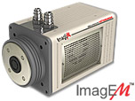
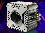
 Electron Multiplying Charge-Coupled Devices (EMCCDs)
By incorporating on-chip multiplication gain, the electron multiplying CCD achieves, in an all solid-state sensor, the single-photon detection sensitivity typical of intensified or electron-bombarded CCDs at much lower cost and without compromising the quantum efficiency and resolution characteristics of the conventional CCD structure.
Product Information
Interactive Flash Tutorials
Full-Frame CCD Operation
Full-frame charge-coupled devices (CCDs) feature high-density pixel arrays capable of producing digital images with the highest resolution currently available. This popular CCD architecture has been widely adopted due to the simple design, reliability, and ease of fabrication. Instructions for operation of the tutorial appear beneath the applet window.
The pixel array illustrated in the full-frame CCD above consists of a parallel shift register, onto which images are optically projected by means of a camera lens or microscope optical train. In this configuration, all of the photodiodes in the pixel array collectively act as the image plane and are available for detecting photons during the exposure period. This is illustrated in the tutorial as the area in which the image slowly formed. The speed in which the CCD collects image data is adjustable with the Image Acquisition Delay slider. A miniature portion of the total image is contained in each pixel element, which consists of four photodiodes masked with red, green, and blue colored filters. The image presented in the upper right-hand corner of the tutorial is an actual high-magnification photomicrograph of a single pixel element.
After photons composing the image have been collected by the pixel elements and converted into electrical potential, the CCD undergoes readout by shifting rows of image information in a parallel fashion, one row at a time, to the serial shift register (illustrated as a series of gray-scale elements at the bottom of the pixel array). The serial register then sequentially shifts each row of image information to an output amplifier as a serial data stream. This action is controlled by the CCD Speed slider in the tutorial. Use the mouse cursor to shift the slider to the left to observe the CCD at slower shift speeds, or to the right for faster speeds. The entire process is repeated until all rows of image data are transferred to the output amplifier and off the chip to a analog-to-digital signal converter integrated circuit. Reconstruction of the image in a digital format yields the final photograph or photomicrograph.
Full-frame CCD architecture has what is termed a 100 percent fill factor, meaning that the entire pixel array is used to detect incoming photons during exposure to the object being imaged. CCDs of this type typically have square pixel dimensions to avoid image distortion and are fabricated with pixel sizes ranging from 7 to 24 microns in arrays containing up to 6 million pixels. Due to the fact that the pixel array is used for both image detection and readout, a mechanical shutter or synchronized strobe illumination scheme must be used to prevent smearing for most exposure periods.
Contributing Authors
Mortimer Abramowitz - Olympus America, Inc., Two Corporate Center Drive., Melville, New York, 11747.
Kevin John, Stephen P. Price, and Michael W. Davidson - National High Magnetic Field Laboratory, 1800 East Paul Dirac Dr., The Florida State University, Tallahassee, Florida, 32310.


