Image Galleries
Featured Article
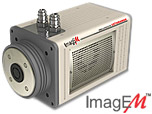
 Electron Multiplying Charge-Coupled Devices (EMCCDs)
By incorporating on-chip multiplication gain, the electron multiplying CCD achieves, in an all solid-state sensor, the single-photon detection sensitivity typical of intensified or electron-bombarded CCDs at much lower cost and without compromising the quantum efficiency and resolution characteristics of the conventional CCD structure.
Product Information
Interactive Flash Tutorials
Microlens Arrays
Microlens arrays (also referred to as microlenticular arrays or lenslet arrays) are used to increase the optical fill factor in some CCDs, which suffer from reduced aperture due to metal shielding. These tiny lens systems serve to focus and concentrate light onto the photodiode surface instead of allowing it to fall on non-photosensitive areas of the device.
The tutorial consists of a schematic diagram of a interline CCD pixel pair, one equipped with a microlens to concentrate light into the photodiode, while the other must absorb incident light rays without the benefit of optical assistance from a microlens. Incident photons that strike the microlens are directed into the photodiode by refraction through the glass or polymer comprising the microlens. The photodiode without a microlens collects a significantly lower portion of incoming photons, because those that impact on shielded areas (the exposure gate and neighboring structures) are not useful in charge integration. Two sliders control incoming photon parameters. The Illumination Wavelength slider is used to control the color (wavelength) of photons striking the CCD, and the Photon Intensity slider can increase or decrease the number of photons in the applet.
Contributing Authors
Mortimer Abramowitz - Olympus America, Inc., Two Corporate Center Drive., Melville, New York, 11747.
Clay Krauterbluth and Michael W. Davidson - National High Magnetic Field Laboratory, 1800 East Paul Dirac Dr., The Florida State University, Tallahassee, Florida, 32310.


