
Image Galleries

Featured Article
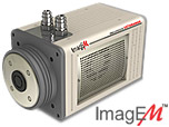 Electron Multiplying Charge-Coupled Devices (EMCCDs)
By incorporating on-chip multiplication gain, the electron multiplying CCD achieves, in an all solid-state sensor, the single-photon detection sensitivity typical of intensified or electron-bombarded CCDs at much lower cost and without compromising the quantum efficiency and resolution characteristics of the conventional CCD structure.
Product Information
Review Articles
Concepts in Digital Imaging Technology
CCD Saturation and Blooming
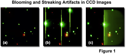
Saturation and blooming are related phenomena that occur in all charge-coupled device (CCD) image sensors under conditions in which either the finite charge capacity of individual photodiodes, or the maximum charge transfer capacity of the CCD, is reached. Once saturation occurs at a charge collection site, accumulation of additional photo-generated charge results in overflow, or blooming, of the excess electrons into adjacent device structures. A number of potentially undesirable effects of blooming may be reflected in the sensor output, ranging from white image streaks and erroneous pixel signal values (as illustrated in Figure 1) to complete breakdown at the output amplification stage, producing a dark image.
The charge capacity of an image sensor can be limited by either the individual photodiode characteristics (pixels) or the CCD itself, and is defined by the maximum amount of charge that the image sensor can collect and transfer while still maintaining all of its design performance specifications. This capacity limit is termed the saturation charge level, and when this limit is reached, the pixel or CCD is described as being saturated. Exceeding the saturation level results in the generation of blooming artifacts in captured images. Blooming refers to the overflow of excess confined photo-generated charge from a photodiode well into adjacent structures when the maximum well charge capacity is exceeded. The extent of degradation of adjacent image areas as a result of blooming depends on the CCD fabrication details and the degree of charge overflow. Since the occurrence of blooming is triggered by the saturation condition, it is useful to know the detector output voltage corresponding to its maximum charge capacity. This value, defined as the saturation voltage, represents the effective maximum output voltage of the CCD, and is calculated by multiplying the charge capacity by the charge-to-voltage conversion factor (the output sensitivity of the imaging device), as follows:
Vsat = Nsat × (dV/dN)
where V(sat) is the saturation voltage, N(sat) is the charge capacity, and dV/dN represents the charge-to-voltage conversion factor. This latter variable, which is equivalent to the CCD output sensitivity, is simply a ratio stating the change in output voltage for a given quantity of charge transferred onto the charge detection node of the device.
The amount of charge that can be accumulated in an individual pixel is defined by its full well capacity, and depends primarily on the pixel dimensions. Other design factors can also affect pixel charge capacity, including the requisite operational voltages and whether or not multi-pinned phase (MPP) technology is employed to reduce dark current. Because of differences in CCD design architecture, various mechanisms of charge transfer may be active. In addition, the operation schemes employed with different designs differ significantly in details, such as clocking patterns, and as a result the onset of saturation conditions is not characterized identically in all CCDs. Saturation can be theoretically defined on the basis of full well conditions, but the complexity of potential well physics prevents simply considering well capacity as a performance parameter. It is common for CCD imagers to exhibit some effects of approaching a saturation condition before full well capacity is actually reached. As an example, the apparent sensitivity of a CCD may decrease with increasing average signal level because changes in charge transfer dynamics reduce the probability of electron trapping in potential wells nearing saturation. A possible result is increasing deviation by the CCD from linear response, even before blooming artifacts appear. With high-performance sensors intended for scientific applications, considerable effort is made to ensure a linear relationship between incident photon level and output signal from the CCD.
If pixel saturation is considered to correspond to full well conditions, one early indication of its occurrence is the observation that increasing specimen illumination intensity does not result in additional signal detection; further charge accumulation may subsequently produce visible blooming artifacts. The quantitative capabilities of the CCD are compromised when its response deviates from linearity, and, as previously described, this may occur for some sensor designs before any visual effects of blooming are apparent. When operation is restricted to only the linear portion of full well capacity (linear full well), the CCD performs as a photometric detector suitable for quantitative measurements. Because of the variety of CCD design types, and different practical definitions of saturation and blooming, a number of control measures may be employed. In practice, it is more important that the effects of saturation are avoided than that the condition is precisely defined for the specific CCD system being utilized.
It is likely, for many CCD cameras, that the system will begin operating outside the range of linear response before the phenomenon of blooming occurs. Although a variety of different mechanisms are available to minimize the effects of blooming in charge-coupled devices, depending on the specific CCD design and type of application, it is usually preferable to recognize and avoid saturation conditions rather than to rely on antiblooming measures. One factor to be considered is the proper operation of the camera gain control, which can be adjusted so that the full bit depth of the analog-to-digital converter does not span more than the linear full well capacity of the CCD. When this setting is properly executed, the full 12, 14, or 16-bit capabilities of a high-performance camera can be utilized for photometric applications without approaching the maximum full well pixel capacity.
Certain anomalies in noise characteristics provide another indication of the approach to sensor saturation. Under illumination conditions in which the CCD is operating in the shot noise dominated regime, as light intensity and signal increase, random noise increases as the square-root of the signal. At some illumination level approaching the onset of full well, the positive random noise variations, which add to signal level, begin to be clipped, or smoothed. This phenomenon, termed noise clipping, causes the average noise level to begin to decrease, even while signal is increasing (see Figure 2(a). At full well conditions, the noise decreases suddenly as charge is spread among neighboring pixels (blooming), while the signal remains stable. When photon transfer curves are constructed, plotting noise as a function of average signal, noise increases with signal at a slope governed by the dominant noise regime (see Figure 2(b)). Full well conditions, and the onset of blooming, results in an obvious break in the slope of the curve.
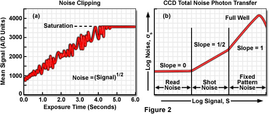
Saturation and blooming normally occur at a relatively high signal levels within the fixed-pattern noise regime of the CCD (Figure 2(b), in which noise is directly proportional to signal. Signal-to-noise ratio (SNR) is likewise proportional to signal in this noise regime, and this can significantly limit camera performance if the full dynamic range (up to the full well limit) is utilized. Scientific grade camera systems generally employ flat-fielding techniques to remove pixel nonuniformity noise, enabling imaging to be performed over an expanded shot noise limited regime. Within this noise regime, image SNR increases in proportion to the square-root of full well, with much greater potential for achieving high image quality, especially when high well-capacity sensors are employed. By removing pixel nonuniformity, a CCD sensor can be utilized over a dynamic range that extends at least up to the linear full well while still operating within the desired shot noise limited regime, and while maintaining high image quality up to the point at which blooming artifacts appear.
Among the possible mechanisms for control of blooming, the most common approach is to include specific CCD design features for that purpose during fabrication of the sensor. In general, the effects of blooming can be reduced significantly by incorporating antiblooming structures near charge collection wells in the CCD to provide a safe path for excess charge removal that does not corrupt image data. The two most common types of structure incorporated into pixels to function as "discharge overflow" drains for bloomed charge (or blooming charge) are the vertical overflow drain (VOD) and the lateral overflow drain (LOD). If other options are available to limit pixel saturation, antiblooming structures are not typically implemented in camera systems intended for scientific use, due to a significant sacrifice in quantum efficiency and well capacity. The reduction in sensitivity due to inclusion of these structures in the CCD architecture limits their utility for low light imaging, such as fluorescence microscopy, but they are an essential option for some imaging applications.
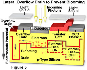
Lateral and vertical antiblooming drains differ significantly in structure and performance characteristics. Simplified details of the two general architecture types are illustrated in Figures 3 and 4. Lateral antiblooming structures are fabricated such that an antiblooming gate, or overflow gate, is positioned adjacent to the pixel's charge collection site where it can be biased to allow excess charge to overflow into a reverse-biased diode and be drained to ground before blooming can occur (as illustrated in Figure 3). In some designs, the lateral drains run the length of the parallel shift registers where they are shared by all pixels in one or more adjacent vertical columns, depending upon their spacing. A charge drain can be located adjacent to every second pixel column, and the antiblooming gate length and drain area are designed to be as small as possible to maintain the maximum well area and capacity. Because the lateral antiblooming structure occupies approximately 30 percent of the pixel area, the proportion that is light sensitive (referred to as pixel fill factor) is reduced to around 70 percent, compared to the potential 100-percent active area that is possible in CCDs without built-in antiblooming structures.
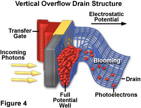
The vertical overflow type of antiblooming structure is positioned directly beneath the charge collection well, and is designed to allow excess charge to overflow directly into the substrate rather than moving laterally into a drain channel, as illustrated in Figure 4. The vertical antiblooming device architecture is based on different epitaxial layer structure than the lateral design, and utilizes controlled distribution of implanted ions in the n-buried channel to provide a path for blooming charge to pass from the center of the channel into the substrate. The charge collection well is maintained by a built-in electrostatic potential barrier to the biased substrate, but that barrier is designed to operate at a level that is lower than the barriers between pixels. When the collected charge exceeds the substrate barrier potential it overflows vertically into the silicon where it is swept away by the substrate bias, rather than overflowing into adjacent pixels. Application of the vertical antiblooming architecture necessarily produces a device with a very shallow photosensitive region, and charge that is generated at greater depth than a few micrometers is lost to substrate absorption. One result is low sensitivity in the near-infrared spectral region, due to the minimal charge generation near the CCD surface for longer wavelengths.
Any type of antiblooming structure incorporated into the CCD architecture involves some reduction in sensor performance, and drain devices containing lateral or vertical overflows present specific advantages and disadvantages. An incidental benefit of either antiblooming scheme is that the feature can be employed as an electronic shutter mechanism for exposure control, making mechanical shutters unnecessary with some CCD imaging systems. Electronic shuttering is a much more precise and reliable method of exposure control than are mechanical devices, and the technique greatly enhances the versatility of camera operation, particularly in computer controlled imaging systems and at high frame rates. Although they have a negative effect on quantum efficiency and sensitivity, antiblooming devices are extremely valuable when the brightness range of a single image frame spans many orders of magnitude, especially if the alternative is not recording the image at all or having it spoiled by blooming artifacts that obliterate important image areas.
In addition to the low sensitivity of the vertical overflow device, especially in certain spectral regions, other typical disadvantages associated with this type of architecture include reduced well capacity and the resulting lower dynamic range, compared to sensors having lateral overflow structures. Although the charge collection efficiency of the vertical overflow drain design is exceptional due to the lack of field-free areas into which charge can diffuse, the overall quantum efficiency is low, with a typical peak value of approximately 25 percent. Additionally, the incorporation of vertical structures in a CCD preclude thinning and backside illumination methods, and the device complexity adds to fabrication costs.
Lateral overflow drain structures are more efficient in preventing blooming than the vertical design, and are used in the most demanding applications. Because the lateral drain is implemented on the surface of the silicon chip at the level of the other circuit structures, it can be fabricated at lower cost than the vertical configuration. The primary disadvantage of the lateral overflow drain architecture is that the area occupied by the drains reduces the active area of the pixels by a significant proportion. As discussed previously, surface antiblooming gates reduce the pixel light-sensitive area by approximately 30 percent, producing an active area specification (fill factor) of 70 percent. The reduced fill factor, accompanied by much lower electron well depth, result in lower light sensitivity compared to a similar sensor without antiblooming protection. In addition, the gaps between light sensitive areas occupied by the overflow structures lowers the effective spatial resolution of the CCD.
In low-light imaging situations requiring maximum sensitivity, antiblooming device protection is usually not desirable, and other alternatives are employed when possible. In scientific imaging systems, which usually do not incorporate antiblooming devices, special clocking techniques are sometimes utilized in multi-phase CCDs as a useful technique for eliminating blooming, although this approach is less effective at higher frame rates, and is most appropriate at low illumination levels. The methodology, referred to as clocked antiblooming, involves partially clocking the CCD during integration to prevent any pixel from reaching the saturation condition. During the integration interval, two of the three phases are alternately switched as saturation is approached, forcing excess charge into the silicon-silicon dioxide interface where it recombines with holes (the third phase does not participate in the clocking process and serves only as a barrier). By repeating the switching process at a sufficient rate to prevent charge from overflowing into neighboring pixels, blooming artifacts are avoided. Charge is recombined at the silicon-oxide interface at the same rate as it is generated, allowing excess charge in pixels nearing saturation to be eliminated, while charge in non-saturated pixels is maintained for read-out. At the end of the integration period, the camera shutter is closed and the accumulated charge is transferred and read out as usual.
Although CCD sensors respond linearly over a wide dynamic range, when full well conditions are reached under high average intensity, nonlinear response will become a problem. Note that good linearity may extend beyond full well in situations where a small area of the image field is overexposed, but is surrounded by a lower average intensity level. If overall illumination is sufficiently bright, however, the CCD response becomes nonlinear and saturation occurs, accompanied by blooming over the entire array. Saturation exists when an increase in intensity produces no further change in recorded signal. With excessive average intensity over the full pixel array, the onset of nonlinear response and full well occur at the same signal level.
Nonlinear sensor response is usually associated with high illumination conditions that produce saturation. Depending upon the sensor, the deviation from linear behavior may also occur under extremely low illumination levels, and in principle, the response in these regions of nonlinearity can be calibrated if required. The best practice, however, is to limit exposures to the region of linearity for the particular sensor being utilized, especially when saturation is possible, since the onset can be rapid and difficult to predict. Among operational measures that can be taken to avoid CCD saturation in high illumination conditions is to make several shorter exposures that are equivalent in combined duration to the desired total integration interval. The multiple short-exposure images can be digitally combined during processing, although in some applications consideration must be given to the implications of the different signal-to-noise factors that prevail when combining several short exposures compared to a single image integration over a longer interval.
An additional form of saturation that must be considered in some situations results from the fact that, in general, charge wells in all CCDs can hold more than they can effectively transfer. The saturation effects observed in many instances are caused by the approach of the maximum charge transfer limit for the CCD. In an extreme condition, such as very high-level exposure of a sensitive camera that is optimized for low-illumination applications, many pixels in the array may reach saturation, resulting in output stage saturation. The use of extensive pixel binning can multiply the charge transfer requirements, and in some circumstances, the charge overload at the CCD output node can produce a collapse of the output amplification chain and a complete loss of image signal.
Contributing Authors
Thomas J. Fellers and Michael W. Davidson - National High Magnetic Field Laboratory, 1800 East Paul Dirac Dr., The Florida State University, Tallahassee, Florida, 32310.