
Image Galleries
Featured Article
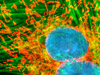
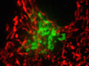
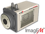 Electron Multiplying Charge-Coupled Devices (EMCCDs)
By incorporating on-chip multiplication gain, the electron multiplying CCD achieves, in an all solid-state sensor, the single-photon detection sensitivity typical of intensified or electron-bombarded CCDs at much lower cost and without compromising the quantum efficiency and resolution characteristics of the conventional CCD structure.
Product Information
Interactive Tutorials
Interactive Flash Tutorials
Conversion Efficiency - Conversion efficiency is one way of describing the relationship between gray levels in software and the related signal levels in an image. The term describes the number of electrons in a CCD that are used to equal an intensity change of one gray level in the software.
Dynamic Range and Detectable Signal Change - The concept of defining the difference between Dynamic Range and Detectable Signal Change is important for understanding the limits of a detector in quantitative imaging. It is also beneficial for designing experiments based on the limits of the available detector and understanding when the detector or the signal itself is the limiting factor in the precision of the results.
Image Processing - Explore the basic concepts of digital image processing applied to specimens captured in the microscope. Techniques reviewed include contrast, color balance, spatial resolution, image sampling frequency, geometric transformation, averaging, measurements, histogram manipulation, convolution kernels, filtering digital images, compression, noise reduction, and binary digital images.
Tools for Digital Imaging - Explore the basic concepts in digital imaging with our illustrated discussions and interactive Flash tutorials. Topics covered include CCD operation, binning, blooming, image capture, dynamic range, electronic shutters, CCD clocking schemes, quantum efficiency, photodiodes, photomultipliers, digital manipulation of images and a wide spectrum of other issues in this emerging field.
Interactive Java Tutorials
Analog-to-Digital Conversion - The output from a majority of present-day video sensors and cameras, such as charge-coupled devices (CCDs) and vidicon tubes, is still in the analog form. With analog signals, the first stage in digital image processing systems is an electronic digitizer, the analog-to-digital (A/D) converter, or ADC, utilized to convert the analog output of the camera or sensor to a sequence of integer numerical values.
Resolution (Airy Disk/Intensity Profile) - The ultimate resolution of a charge-coupled device image sensor is a function of the number of photodiodes and their size relative to the image projected onto the surface of the imaging array by the microscope optical system. When attempting to match microscope optical resolution to a specific digital camera and video coupler combination, use this tutorial for determining the minimum pixel density necessary to adequately capture all of the optical data from the microscope.
Streak Lifetime Imaging (FLIM) Camera - An optical image with intensity information at every pixel is converted to a streak image with spatial information displayed on the horizontal axis and time on the vertical axis. Every point in a streak image provides information representing intensity, location, and time. The CCD detector creates a point-by-point map of this information for evaluation.
CCD Noise Sources - Innovations in silicon based CCD technology have created many varieties of CCDs. With the quantum efficiency of the traditional front-illuminated CCD reaching about 70 percent and the more advanced back-thinned esign achieving more than 90 percent, detection limits are nearing their theoretical values. Signal detection in modern CCDs is often limited by how much camera noise (due to dark current and readout) must be overcome before the signal is apparent on the CCD. These values determine the camera performance of CCD, especially in low light applications.
EMCCD Temperature Versus Gain - In the case of an EMCCD image sensor, the multiplication gain factor in the multiplication register greatly depends on the temperature. It is obvious that the stabilization of temperature of a sensor becomes a very important issue. This interactive tutorial demonstrates an example the dependence of gain with temperature for an E2V CCD97 CCD. A change of 70 degrees at the CCD changes the EM gain by about 10 times in the tutorial. In addition, as the temperature is decreased, the slope of the change increases. Temperature stability becomes increasingly important at lower cooling temperatures to maintain constant gain in an EMCCD.
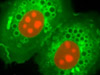
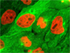
EMCCD Gain - Explore image capture with an EMCCD camera using this interactive tutorial. The live image is displayed in the upper right-hand corner, while the captured image is presented in the lower right, just above the sliders. The EMCCD acquires photons in the Image Area and transfers them to the Storage Area prior to readout. All of the specimens are labeled with a green or yellow fluorescent protein (green signal). Noise is represented as red (dark current) or blue (multiplier noise) photoelectrons. The tutorial is activated upon clicking the Capture button and can be halted at any instant using the Pause button. The Gain Level slider controls the amount of multiplication in the Gain Register. New specimens can be selected using the pull-down menu.
EMCCD Noise - The performance of electron multiplying CCDs depends on a number of interdependent factors. In addition to factors found in normal CCDs, such as quantum efficiency, full well capacity, dynamic range, dark current (and it's related dark noise), and readout noise, additional factors are involved. Electron multiplication CCDs must be designed with consideration for additional gain related noise sources, multiplication of the dark noise along with the signal, gain ageing effects and the actual impact ionization phenomenon that produces the gain itself.
EMCCD Clocking - This interactive tutorial illustrates the principle of signal multiplication in the charge multiplication register of an electron multiplying CCD. When a signal electron charge is transferred from stage to stage, the signal charge is accelerated through a high electric field generated under the multiplication gate by applying a high voltage (30 to 40 volts) to each multiplication electrode (multiplication gate). This high voltage is much greater than the normal horizontal transfer electrode voltage, and it generates an occasional extra electron-hole pair. This effect is called an impact ionization event. The probability of such an event is very small, typically about 1.0 to 1.6 percent at each stage. Electrons are multiplied from stage to stage repeatedly in the gain register and high multiplication gain is achieved. Normally, there are 400 to 600 stages in the gain register.
Two Phase CCD Clocking - A two phase charge transfer CCD clocking scheme employs four gates for each pixel, with adjacent gates connected together as pairs. The two phase CCD scheme requires a more complex clocking arrangement than that described for the four phase and three phase CCD architectures. The shift register illustrated in this tutorial includes two pixel elements, for a total of eight gates aligned along a common axis to form a column. Each gate pair is connected to an alternate clock line and one of the gates in each pair is designed with an increased n-type doping level beneath the gate. When voltage is applied to the gate pair, the gate having the increased doping level has a more positive potential, which increases the depth of the charge storage area and results in a "step" in the potential energy profile.
Three Phase CCD Clocking - Charge transfer through CCD shift registers occurs after integration in order to relocate accumulated charge information to the sense amplifier, which is physically separated from the parallel pixel array. Several clocking schemes, including the three phase technique illustrated in this interactive tutorial, are utilized to transfer charge from the collection gates to the output node.
Four Phase CCD Clocking - A four phase CCD incorporates four individual polysilicon gate electrodes in each pixel cell, each of which requires a separate input clock signal to properly transport accumulated charge. The shift register illustrated in the tutorial includes two pixel elements, for a total of eight gates aligned along a common axis to form a column. The nature of electrostatic forces in the silicon substrate beneath the gates is determined by the voltage level applied to a particular gate by the clock input signal. High level voltages induce the formation of a potential "well" beneath the gate, whereas low level voltages form a potential barrier to electron movement.
Time Delay Integration Scanning - Time Delay Integration (TDI) is an imaging process in which a frame transfer image sensor produces a continuous video image of a moving two-dimensional object. The translation of the specimen is exactly synchronized with the vertical charge transfer of each pixel on the CCD. This process offers on-the-fly integration of signal intensity of a moving object. By altering the speed of image motion and the related charge transfer, total integration time can be regulated. In addition, by providing more or less pixels in the vertical direction, total integration time can be adjusted at a fixed specimen speed.
TDI Drum Scanning - The Time Delay Integration (TDI) CCD system is an ideal tool for capturing images of rotating objects or rapidly moving specimens, and is thus widely utilized in line scan cameras for industrial robots and similar applications. This interactive tutorial explores capturing images of rapidly moving objects using characters printed on a virtual drum by a CCD operating in a combination of frame and TDI mode.