
Image Galleries
Featured Article
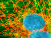
 Electron Multiplying Charge-Coupled Devices (EMCCDs)
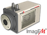
By incorporating on-chip multiplication gain, the electron multiplying CCD achieves, in an all solid-state sensor, the single-photon detection sensitivity typical of intensified or electron-bombarded CCDs at much lower cost and without compromising the quantum efficiency and resolution characteristics of the conventional CCD structure.
Product Information
Review Articles
Review Articles
Basic Properties of Digital Images - Continuous-tone images are produced by analog optical and electronic devices, which accurately record image data by several methods, such as a sequence of electrical signal fluctuations or changes in the chemical nature of a film emulsion that vary continuously over all dimensions of the image. In order for a continuous-tone or analog image to be processed or displayed by a computer, it must first be converted into a computer-readable form or digital format. This process applies to all images, regardless the origin and complexity, and whether they exist as black and white (grayscale) or full color. A digital image is composed of a rectangular (or square) pixel array representing a series of intensity values and ordered through an organized (x,y) coordinate system.
Introduction to Digital Imaging in Microscopy
Part I: Basic Imaging Concepts - This article describes the fundamentals of digital image acquisition, spatial resolution, contrast, brightness, bit depth, dynamic range, CCD fundamentals, and performance measures as well as image display and storage issues. Starting with a historical perspective, the conversion of images from analog to digital format is reviewed followed by discussions of the contrast transfer function, histograms, quantum efficiency, noise, cooling, binning, and linearity.
Part II: Basic Microscopy Concepts - The primary considerations in imaging living and fixed cells in the microscope with a digital camera are detector sensitivity (signal-to-noise), the required speed of image acquisition, and specimen viability. The relatively high light intensities and long exposure times that are typically employed in recording images of fixed cells and tissues (where photobleaching is the major consideration) must be strictly avoided when working with living cells. In virtually all cases, live-cell microscopy represents a compromise between achieving the best possible image quality and preserving the health of the cells. Rather than unnecessarily oversampling time points and exposing the cells to excessive levels of illumination, the spatial and temporal resolutions set by the experiment should be limited to match the goals of the investigation.
Concepts in Digital Imaging Technology
Electron Multiplying Charge-Coupled Devices (EMCCDs) - By incorporating on-chip multiplication gain, the electron multiplying CCD achieves, in an all solid-state sensor, the single-photon detection sensitivity typical of intensified or electron-bombarded CCDs at much lower cost and without compromising the quantum efficiency and resolution characteristics of the conventional CCD structure.
Electronic Imaging Detectors - The range of light detection methods and the wide variety of imaging devices currently available to the microscopist make the selection process difficult and often confusing. This discussion is intended to aid in understanding the basics of light detection and to provide a guide for selecting a suitable electronic detector (CCD or video camera system) for specific applications in optical microscopy.
Anatomy of a Charge-Coupled Device - Digital image sensor technology is centered around the semiconductor charge-coupled device, which is fabricated in a manner similar to that used in the production of integrated circuits ranging from microprocessors to memory chips. This section discusses common features of CCD anatomy and the basic principles of device operation.
Binning - Pixel binning is a clocking scheme used to combine the charge collected by several adjacent CCD pixels, and is designed to reduce noise and improve the signal-to-noise ratio and frame rate of digital cameras. The binning process is performed by on-chip timing circuitry that assumes control of the serial and parallel shift registers prior to amplification of the CCD analog signal.
CCD Saturation and Blooming - Saturation and blooming are related phenomena that occur in all CCD image sensors under conditions in which either the finite charge capacity of individual photodiodes, or the maximum charge transfer capacity of the CCD, is reached. Once saturation occurs at a charge collection site, accumulation of additional photo-generated charge results in overflow, or blooming, of the excess electrons into adjacent device structures. A number of potentially undesirable effects of blooming may be reflected in the sensor output, ranging from white image streaks and erroneous pixel signal values to complete breakdown at the output amplification stage, producing a dark image.
Dynamic Range - In a charge-coupled device (CCD) or complementary metal oxide semiconductor (CMOS) image sensor, dynamic range is typically specified as the maximum achievable signal divided by the camera noise, where the signal strength is determined by the full-well capacity, and noise is the sum of dark and read noises. As the dynamic range of a device is increased, the ability to quantitatively measure the dimmest intensities in an image (intrascene performance) is improved. The interscene dynamic range represents the spectrum of intensities that can be accommodated when detector gain, integration time, lens aperture, and other variables are adjusted for differing fields of view.
Quantum Efficiency - The quantum efficiency of a charge-coupled device (CCD) is a property of the photovoltaic response defined as the number of electron-hole pairs created and successfully readout by the device for each incoming photon. This property is especially important for low-light imaging applications such as fluorescence microscopy where illumination is sparse and secondary emission photon wavelengths are often in the 375-550 nanometer range and have a relatively high absorption coefficient.
CCD Noise Sources and Signal-to-Noise Ratio - Charge-coupled device (CCD) sensors have numerous advantages over photographic film in scientific imaging applications such as astronomy and optical microscopy. By directly producing images in digital format, suitable for immediate computer processing, CCD-based image capture systems are ideally suited to a wide range of current microscopy and image analysis methods. In particular, the much greater sensitivity of such sensors compared to film is invaluable in low-light techniques, for which every available signal photon may be significant. Noise, arising from a variety of sources, is inherent to all electronic image sensors, and careful control of noise components, both in the design and operation of the CCD system, is necessary to ensure that the signal level relative to noise is adequate to allow capture of accurate image information. For any electronic measuring system, the signal-to-noise ratio (SNR) characterizes the quality of a measurement and determines the ultimate performance of the system.
Charge-Coupled Device (CCD) Linearity - An important characteristic of a scientific imaging system is the linearity in response to incident light, particularly when applied for quantitative photometric analysis. In digital camera systems employing charge-coupled device (CCD) sensors, the fundamental function of the CCD is to convert photons carrying image information into an electronic signal. After digitization, the signal output should ideally be linearly proportional to the amount of light incident on the sensor.
Electronic Shutters - Electronic shutters are employed in charge-coupled devices (CCDs) to control integration time (exposure) of the photodiode array and reduce smear when capturing moving objects in the microscope.
Charge Transfer Clocking Schemes - Charge transfer through CCD shift registers occurs after integration to relocate accumulated charge information to the sense amplifier, which is physically separated from the parallel pixel array. Several clocking schemes, three of which are discussed below, are utilized to transfer charge from the collection gates to the output node.
- Four Phase CCD Clocking - A four phase CCD incorporates four individual polysilicon gate electrodes in each pixel cell, each of which requires a separate input clock signal to properly transport accumulated charge.
- Three Phase CCD Clocking - Three phase CCD clocking improves spatial resolution over that obtained in four phase devices, yet requires only three gates per pixel. This scheme differs from four phase clocking by using only one storage gate and two barrier gates, which allows for faster frame rates and the fabrication of higher density and resolution CCDs.
- Two Phase CCD Clocking - A two phase charge transfer CCD clocking scheme employs four gates for each pixel, with adjacent gates connected together as pairs. Each gate pair is connected to an alternate clock line and one of the gates in each pair is designed with an increased n-type doping level beneath the gate. When voltage is applied to the gate pair, the gate having the increased doping level has a more positive potential, which increases the depth of the charge storage area and results in a "step" in the potential energy profile.
CCD Scanning Formats - Charge-coupled device (CCD) digital imaging sensors are capable of acquiring images in one of three formats: point scanning, line scanning, and area scanning. Each of these formats has specific applications in digital photography and scanning of documents and images.
Full-Frame CCD Architecture - Full-frame charge-coupled devices feature high-density pixel arrays capable of producing digital images with the highest resolution currently available. This CCD architecture has been widely adopted due to the simple design, reliability, and ease of fabrication.
Frame-Transfer CCD Architecture - Frame-Transfer charged coupled image sensors have an architecture similar to that of full-frame CCDs. These devices have a parallel register that is divided into two separate and identical areas, termed the Image and Storage arrays.
Interline Transfer CCD Architecture - Interline charge-coupled device architecture is designed to compensate for many of the shortcomings of frame-transfer CCDs. These devices are composed of a hybrid structure incorporating a separate photodiode and an associated CCD storage region into each pixel element.
Digital Camera Readout and Frame Rates - Recent imaging applications in widefield fluorescence and confocal microscopy have increasingly centered on the demanding requirements of recording rapid transient dynamic processes that may be associated with a very small photon signal, and which often can only be studied in living cells or tissues. Technological advances in producing highly specific fluorescent labels and antibodies, as well as dramatic improvements in camera, laser, and computer hardware have contributed to many breakthrough research accomplishments in a number of fields. As high-performance camera systems, typically employing low-noise cooled charge-coupled device (CCD) detectors, have become more capable of capturing even relatively weak signals at video rates and higher, certain performance factors necessarily take on greater importance. A camera system's readout rate and frame rate are interrelated parameters that are crucial to the ability of the system to record specimen data at high temporal frequency.
Microlens Arrays - Microlens arrays (also referred to as microlenticular arrays or lenslet arrays) are used to increase the optical fill factor in CCDs, such as interline devices, that suffer from reduced aperture due to metal shielding. These tiny lens systems serve to focus and concentrate light onto the photodiode surface instead of allowing it to fall on non-photosensitive areas of the device, where it is lost from the imaging information collected by the CCD.
The MOS Capacitor - At the heart of all charge-coupled devices (CCDs) is a light-sensitive metal oxide semiconductor (MOS) capacitor, which has three components consisting of a metal electrode (or gate), an insulating film of silicon dioxide, and a silicon substrate.
Avalanche Photodiodes - Avalanche photodiodes provide gain by the generation of electron-hole pairs from an energetic electron that creates an "avalanche" of electrons in the substrate.
Photomultiplier Tubes - A photomultiplier tube, useful for light detection of very weak signals, is a photoemissive device in which the absorption of a photon results in the emission of an electron. These detectors work by amplifying the electrons generated by a photocathode exposed to a photon flux.
Proximity-Focused Image Intensifiers - Image intensifiers were developed for military use to enhance our night vision and are often referred to as wafer tubes or proximity-focused intensifiers. They have a flat photocathode separated by a small gap on the input side of a micro-channel plate (MCP) electron multiplier and a phosphorescent output screen on the reverse side of the MCP.
Electron-Bombarded CCDs - The electron-bombarded charge-coupled device (EBCCD) is a hybrid of the image intensifier and the CCD camera, which has just been recently introduced. In this device, photons are detected by a photocathode similar to that in an image intensifier. The released electrons are accelerated across a gap and impact on the back side of a back-thinned CCD.
Sequential Color CCD Sytems - Three-pass sequential color CCD imaging systems employ a rotating color wheel to capture three successive exposures in order to obtain the desired RGB (red, green, and blue) color characteristics of a digital image. The major advantage of this technique is the ability to fully utilize the entire pixel array of a CCD imaging chip, by using one pass for each color.