
Image Galleries

Featured Article
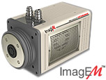 Electron Multiplying Charge-Coupled Devices (EMCCDs)
By incorporating on-chip multiplication gain, the electron multiplying CCD achieves, in an all solid-state sensor, the single-photon detection sensitivity typical of intensified or electron-bombarded CCDs at much lower cost and without compromising the quantum efficiency and resolution characteristics of the conventional CCD structure.
Product Information
Review Articles
Concepts in Digital Imaging Technology
Digital Camera Readout and Frame Rates
Recent imaging applications in widefield fluorescence and confocal microscopy have increasingly centered on the demanding requirements of recording rapid transient dynamic processes that may be associated with a very small photon signal, and which often can only be studied in living cells or tissues. Technological advances in producing highly specific fluorescent labels and antibodies, as well as dramatic improvements in camera, laser, and computer hardware have contributed to many breakthrough research accomplishments in a number of fields. As high-performance camera systems, typically employing low-noise cooled charge-coupled device (CCD) detectors, have become more capable of capturing even relatively weak signals at video rates and higher, certain performance factors necessarily take on greater importance. A camera system's readout rate and frame rate are interrelated parameters that are crucial to the ability of the system to record specimen data at high temporal frequency.
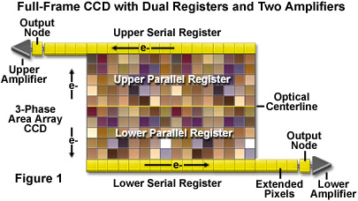
Sensors designed for quantitative imaging, such as those utilized in high-performance optical microscopy cameras, primarily employ a variation of one of three well-known CCD architectures: full frame, frame transfer, or interline transfer. The frame-transfer and interline-transfer formats generally provide faster frame rate capabilities, but manufacturers incorporate a range of structural and clocking enhancements in designs of each type in order to improve performance. Figure 1 illustrates a full-frame CCD sensor designed to achieve high frame rates by use of a split parallel register that can be clocked to transfer charge in two directions toward dual serial registers, each having a separate output amplifier. The frame rate of the sensor can be approximately doubled by this transfer scheme. Several additional modifications of the standard CCD architectures provide similar advantages and are briefly described in the subsequent discussion.
Readout rate is governed by the time required to digitize a single pixel (the serial conversion time) and is defined as the inverse of that value. Because the conversion time for a single pixel is considerably less than one second, typical readout rates have the units of pixels per second. The rate is often stated as a frequency (hertz, Hz), and some camera manufacturers refer to this specification as pixel clock rate or simply clock rate. The frame rate of an imaging system incorporates the exposure time and extends the single pixel readout rate to the entire pixel array. It is defined as the inverse of the time required to acquire an image and to completely read the image data out to the amplifier. This variable is typically stated in frames per second (fps) or in frequency units (Hz). An approximation of frame rate is obtained by taking the inverse of the sum of total pixel digitization time and the exposure (integration) time, as follows:
Approximate Frame Rate (fps) = 1 / [(Npixel / tread) + Texp]
where N(pixel) is the number of sensor pixels being read, and t(read) and T(exp) represent the single-pixel read time and exposure time, respectively. In the equation, the total pixel digitization time for the array is represented by the quotient of the total pixel number divided by the single pixel read time (N(pixel) / t(read)).
Although this simplified expression for calculating frame rate is useful for certain comparison purposes, it omits a variety of other factors that affect the true frame rate achieved in practice, among them the operation mode of the CCD and the required exposure duration relative to frame read time in a given application. The details of the charge collection and transfer mechanisms employed by a particular sensor design, as well as the choice of operation modes, such as binning and reduced-array scanning, are significant in determining the actual imaging frame rate. Furthermore, it is implicit that absolute maximum frame rate is achieved at the expense of exposure duration, and a long exposure time relative to the time required to read out the accumulated charge becomes the limiting factor in such circumstances. In listing camera system specifications, a manufacturer may specify frame rates achieved under "typical" conditions, or in some cases frame rate values are stated for an exposure time of zero for comparison of performance achieved using different scan modes or array sizes.
The true frame rate value is determined by the combined frame acquisition time and frame read time, each of which depends upon operational details specific to the camera system and application. Quantitatively the frame rate is therefore the inverse of the sum of these two variables, as expressed by the following equation:
Frame Rate (fps) = 1 / (Frame Acquisition Time + Frame Read Time)
To obtain an accurate evaluation of the true frame rate, a more detailed accounting of the two primary components is required than is provided by the simplified approximation, which uses the number of pixels divided by the readout rate plus the exposure time. While the frame acquisition and frame read times are conceptually obvious, each encompasses several operational factors that vary with CCD architecture and operating conditions. A number of basic operations typically contribute to the frame acquisition and frame read time intervals, and these are listed and discussed further below.
Frame acquisition time components:
Time required to clear charge from the parallel register prior to beginning integration.
Shutter opening delay in CCDs employing mechanical shutters.
Exposure time.
Shutter closing delay, if any.
Frame read time components:
Time required to clear charge from the serial register prior to beginning readout.
Time required for a parallel row shift times the number of rows in the array.
Serial discard time multiplied by the number of pixels not intended to be read.
Serial conversion (digitization) time per pixel times the number of pixels to be read.
Prior to image acquisition, it is necessary with many CCD sensors to clear the pixel array of charge that may have accumulated prior to exposure, due to dark current, cosmic ray interaction, or other charge-generating events. The time required to clear the entire parallel register (referred to as the parallel clear time) depends upon the charge transfer clocking cycle, which may be repeated several times for complete charge removal. The total time required is equal to the parallel clear time multiplied by the number of clearing cycle repetitions. Elimination of any charge accumulated in the array before starting the actual frame integration reduces the phenomenon of image smear, as well as allowing more precise control of exposure time from frame to frame. Typically, current CCD sensors perform several parallel clearing cycles, but because the charge is discarded and does not have to be digitized, these cycles are faster than normal readout times.
The delay in opening and closing a shutter for control of the exposure times is strictly dependent upon the particular camera system and how it is being operated. Some CCD architectures require the use of an external shutter to shield the array from light during the readout phase of image acquisition. If a mechanical shutter is employed, operation times are likely to be significantly increased. Many high-sensitivity systems are based on frame-transfer CCD architecture, which features separate on-chip storage and integration regions, and these may be operated continuously at high rates without a shutter. The exposure, or integration, time in many optical microscopy applications is commonly the dominant factor contributing to frame acquisition time, and in limiting the maximum frame rate achievable.
Following the data acquisition stage, readout of collected charge occurs through one of several different transfer sequences, depending upon the CCD architecture. In the case of a full-frame device, readout takes place by shifting pixel rows directly from the parallel register into the serial register for transfer to the output amplifier. The frame-transfer CCD differs in that following signal integration, data from the entire image array is shifted to a storage array by simultaneously clocking the two sections in parallel, followed by single-row shifts of data in the store section into the serial register. The shift from the image to the storage array takes place rapidly, and while the storage array is being read out, the image array is available to integrate charge for the next frame. Consequently, the transfer from integration to the storage section is typically not significant in the frame read time determination for frame-transfer devices. Whether the CCD is of the full-frame or frame-transfer design, it may be necessary to clear accumulated charge from the serial register prior to transferring charge from the parallel register. The time required for this operation is referred to as the serial clear time.
After any residual serial register charge is cleared, image readout begins with a clocked sequence of gate potentials that causes all charge packets in the parallel register to be shifted one pixel row toward the serial register, such that the first row (adjacent to the serial register) moves into the serial register. The parallel shift time is the time required to perform a single parallel shift cycle. At this point, the first charge packet in each column is in position to be transferred through the serial register to the output node for processing. Multiplying the parallel shift time by the number of rows in the image array yields the portion of the frame read time accounted for by parallel shifts of pixel rows into the serial register.
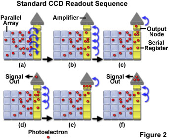
Note that the normal mode of CCD readout is to shift one pixel row into the serial register, then to read each charge packet in that row by performing a series of column shifts in the register, with each pixel's charge being read as it advances to the output node and is collected for amplification and processing. When the entire serial register has been read out by alternating column shifts and pixel read cycles, another parallel shift cycle moves the next row from the array into the serial register. This process is repeated until all charge is shifted out of the parallel register. The major component of the frame read time is the pixel read time, or serial conversion time, which is multiplied by the total number of pixels being read from the image array. Figure 2 represents diagrammatically the normal sequence of accumulating, transferring, and reading out charge from a full-frame CCD.
Illustrated in Figure 2(a) is a truncated parallel CCD pixel array (4 x 4) that has been exposed to light in order to accumulate a charge pattern of photoelectrons (represented by red spheres). Charge in the parallel register is shifted by one row from Figure 2(a) to Figure 2(b), with the edge row of photoelectrons from the parallel register being transferred into the serial register. In Figure 2(c) the first pixel in the serial register is shifted into the output node before being transferred to the amplifier (Figure 2(d)) and output for processing. Simultaneously in Figure 2(d), the charges in the serial register are shifted toward the output node by one pixel. The next charge in the serial register is shifted from the output node to the amplifier in figure 2(e), and the other charges in the serial register are again shifted toward the output by one pixel in Figure 2(f). This sequence is repeated until the entire charge pattern is transferred from the parallel array through the serial register to the amplifier.
Because the pixel read cycle dominates the frame read time, unnecessary pixels should be discarded or ignored rather than being measured. This is the mechanism by which reading a reduced array, or subarray, of a CCD can increase camera frame rate. Pixels transferred off the chip that occur before or after a defined region of interest in the frame can be discarded during the readout cycle. Additional pixels, which also must be discarded, are often positioned adjacent to the output node, extending the serial register size. The serial register of most CCDs has one pixel for each column of the imaging array, plus an additional number (typically 10 - 50) at the end of the register between the data array and the output amplifier (Extended Pixels, see Figure 1). These extra pixels serve both to provide a dark reference level and to help stabilize the serial clock pulse and signal chain before image data reaches the output amplifier.
Discard times may be associated with serial shifts as well as with parallel row shifts, and the total discard time per frame cycle is obtained by multiplying the appropriate discard time by the corresponding number of discards performed. Individual pixels can be ignored (discarded) by performing repeated shifts in the serial register while omitting the pixel read step, resulting in a discrete time value for this step, termed the serial discard time. Entire pixel rows are discarded by programming repeated parallel shifts without performing the serial row readout. Parallel discard time is therefore equivalent to the parallel shift time, and any time saving results from reducing the total number of necessary serial conversions by the number of pixels in the discarded row. In practice, by manipulating the clocking sequences for parallel and serial transfer and for charge readout cycles, portions of the image frame can be programmed for signal output as necessary for a particular application, with corresponding changes in the achievable frame rate.
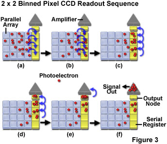
Pixel binning is another mechanism that is utilized to reduce image readout time and increase frame rate in CCD imaging, and is performed in the same manner as subarray display, by programmed variations in clock cycle sequences that control the transfer and digitization of sensor-generated charge packets. The technique of binning combines charge from adjacent pixels during the readout process, thereby improving signal-to-noise ratio and dynamic range of the system. Although an effectively larger pixel size lowers spatial resolution, the reduced number of charge packets to be transferred and digitized allows increased readout speed in conjunction with the improved signal level.
Both parallel and serial binning are possible, and in similarity to reduced-array readout, a charge integration period is performed, but the subsequent clocking sequences for charge transfer and pixel readout differ from those normally programmed. Parallel binning is performed during the readout cycle by clocking two or more parallel transfers into the serial register while holding the serial clocks fixed. The effect is to sum pixel charge from multiple rows into each serial pixel before the serial shift cycle begins. The serial binning process transfers two or more charge packets from the serial register into the CCD output node before the charge is read out. Figure 3 presents a binned readout sequence, in which charge from two parallel transfers is summed in the serial register, followed by summing of two serial pixels into the output node for readout. Each readout cycle thus contains the charge from four adjacent pixels.
Various degrees of pixel binning can be utilized, and this is indicated by specifying the number of pixels being combined in the parallel and serial shift directions (termed binning factor, with a value of 1 indicating no binning). For example, a 3 x 3 binning factor specifies that three charge packets are summed into each well of the serial register by parallel shift repetitions, followed by three serial shift repetitions for each cycle of charge readout. Thus, for 3 x 3 binning, each charge packet digitized for image display or quantitative analysis represents nine adjacent pixels of the CCD array. Practically, any combination of parallel and serial binning factors may be programmed as a readout mode provided that the sum of charge from the binned pixels does not exceed the full well capacity of the device. In order to accommodate charge summing and to maintain charge transfer efficiency, pixels in the serial register are typically designed to have higher well capacity than those in the parallel register. With regard to the effect of binning on the frame read time, parallel shift and serial conversion times are not affected, and the increased readout speed results simply from the reduction in the number of charge packets (combined pixels) subject to processing through the readout node.
To summarize the factors that contribute to frame acquisition time and frame read time, and which therefore determine a camera's true frame rate, the following expressions can be employed:
Frame Acquisition Time = (TPR × Nclear) + Topen + Texp + Tclose
where T(PR) and N(clear) are the time required to clear the parallel register and number of clear cycles performed, and T(open), T(exp), and T(close) represent the shutter opening delay time, the exposure time, and the shutter closing delay time, respectively.
Frame Read Time = TSR + (Trow × Nrow) + (TSD × Ndiscard) + (tread × Nread)
where T(SR) represents the time required to clear the serial register, T(row) and N(row) are the time required for a parallel row shift and the number of rows in the array, T(SD) and N(discard) are the serial discard time and the number of pixels not being read, t(read) is the serial conversion time per pixel and N(read) represents the number of pixels to be read. This latter number is, at maximum, the total pixel array size, and is reduced in accordance with subarray readout and/or pixel binning operations.
Although the frame acquisition and frame read times combine in determining CCD frame rate, the interrelationship may not be simply additive because in different operation modes and with various CCD architectures, portions of the two processes overlap to different degrees. The architecture design employed in the CCD sensor affects whether the processes of integration and readout must take place sequentially or can occur simultaneously, and in different circumstances, frame rates may have limits imposed by either the exposure time or readout time. In frame-transfer devices, during the data collection interval the clock voltages are not being cycled for charge transfer between imaging and storage sections. However, data previously collected and held in the storage region of the chip can be clocked and transferred at will while signal collection occurs concurrently in the image section. Frame-transfer sensors, consequently, may be operated in several different modes with respect to timing of exposure and readout sequences. Interline-transfer CCDs share a number of the performance attributes of frame-transfer devices due to their also incorporating a storage area, which is arranged, not as a separate storage array, but as columns of masked pixels alternating with columns of active unmasked pixels. The alternating columns of imaging and storage pixels across the parallel register allow signal integrated in the active columns to be shifted quickly under the interline mask, where it is read out to the serial register while charge for the next frame is being integrated in the unmasked pixel columns.
As previously discussed, the relationship between frame rate and the combined time required for acquiring and reading out photon-generated charge in a CCD system depends in part on the exposure and readout modes employed by the CCD. In general, the charge integration phase of image acquisition is carried out in the same manner regardless of the camera's operating mode, and the selection of functions such as subarray image output or pixel binning can provide increased frame rates primarily due to reductions in the frame read time. The time required to clear charge from the CCD registers, and the shift times are sufficiently short that they do not have a major effect on readout rate, which is instead dominated by the pixel read time (serial conversion time).
Individual charge packets are shifted through both the parallel and serial registers under the influence of repeated cycles of clock signals applied to the CCD electrodes. Each pixel is typically driven by three electrodes that permit three-phase clock cycles, in which corresponding electrodes of each pixel are connected in parallel and produce the same charge-transfer effect for every pixel being clocked. A single cycle of the three clock phases produces either a one-row (vertical) shift in the parallel register or a one-column (horizontal) shift in the serial register. Changes in operating mode, such as selection of subarray scanning or various binning factors, are effected by modifying the clock cycle sequences applied to the electrodes. In the selection of a camera system, the degree to which the timing of clock sequences can be controlled in operation of the camera may be a determining factor in the suitability of the system for a particular application.
Because the interrelationship of exposure time and read time is critical in determining camera frame rate, those two variables are often illustrated in timing diagrams for different operating modes supported by a particular CCD architecture. High-performance camera systems typically employ frame-transfer or interline-transfer sensors to enable the fastest frame rates and continuous imaging without the necessity of a mechanical shutter to control exposure times. Because these CCD designs include both a light-sensitive sensor area and a storage area that is shielded from light and used for frame transfer to the serial register, the two processes of exposure and readout can overlap in time. Camera systems may offer selectable exposure and readout modes, which are categorized as non-overlap and overlap modes on the basis of whether the two operations are performed independently in sequence, or simultaneously. Other systems exercise control of these variables in a different manner, or in combination with other features. For example, clocking modes may be determined automatically by camera firmware to maximize frame rate, utilizing overlapped or non-overlapped exposure-readout sequences as required, or may be set to optimize sensitivity without regard to high frame rate. High-sensitivity operation typically requires non-overlapped operation regardless of exposure time.
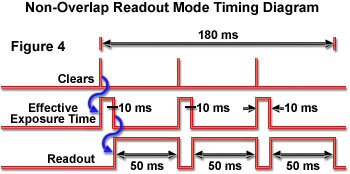
When a CCD is operated in non-overlap mode, any exposure time can be specified and fully completed, with readout occurring in sequence when the exposure has ended. A timing diagram illustrating this exposure-readout mode is presented in Figure 4. In non-overlap mode, the same cycle is repeated for each frame in a sequence; the CCD is cleared of residual charge, charge is integrated for the specified exposure time, the charge is shifted from the light-sensitive array to the masked storage array (separate storage section or interline array), and finally charge is read out. Depending upon specific circumstances, the exposure time may be shorter or longer than the read time, and the total time per frame is the sum of the two intervals (in the absence of mechanical shutter delay), since clearing time and the time required to shift data to the storage array are very rapid and not significant in determining frame rate. This operation mode provides similar performance to that of conventional full-frame device architecture. The timing diagram (Figure 4) illustrates the exposure and readout time sequence for a series of three image frames. Using the arbitrary times shown in the example, 10 millisecond (ms) exposure and 50 millisecond frame read time, the total time to acquire three frames is 180 milliseconds (3 x 10 ms + 3 x 50 ms). The corresponding frame rate is therefore 16.7 frames per second (3 frames/0.180 second).
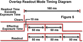
Overlap mode is utilized in applications requiring the recording of dynamic processes, in which continuous imaging is necessary to provide adequate temporal resolution. To maximize the proportion of time devoted to data collection, the CCD is operated continuously (100-percent duty cycle). After the initial exposure, data are shifted to the frame transfer array, and the next exposure interval begins immediately, while readout occurs for the previous frame. This sequence continues, with the timing from frame to frame determined by either the exposure time or the frame read time, depending upon which is longer. The minimum exposure time is therefore equivalent to the frame read time. In situations in which the programmed exposure time is less than the readout time, the first frame in a sequence is exposed for the exact time programmed, with subsequent frames exposed for the readout time. The sequence timing is in effect controlled by the longer-duration readout cycle. Figure 5 illustrates a timing diagram for overlap mode operation with a 10-millisecond programmed exposure time, and CCD readout time of 50 milliseconds, as used in the previous (non-overlap mode; Figure 4) example. The total time required to acquire 3 frames in this mode is 160 milliseconds, calculated on the basis of one 10-millisecond exposure followed by two 50-millisecond exposures, which overlap the three readout cycles of 50 milliseconds each (10 ms + 3 x 50 ms). Operating in overlapped mode results in a reduction in time of 20 milliseconds for a three-frame sequence, and a corresponding frame rate of 18.8 frames per second (3 frames/0.160 second). In this type of sequence, the first frame is exposed for a shorter time than the succeeding ones, and will generally not match in image intensity.
When the programmed exposure time is less than the frame read time, the following general expression can be used to calculate the total time required to capture a specified number of frames (N):
TN = (Tread × N) + Texp
where T(N) is the total time required to capture a sequence of N frames, T(read) is the single-frame read time, and T(exp) represents the programmed exposure time.
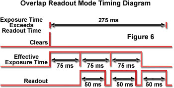
A second possible timing variation occurs during operation in overlap mode when exposure time is greater than frame read time, and therefore controls the timing of sequential frames. As a result, each frame in a sequence is exposed for the exact time specified in the system control software, and all images are of equal intensity. As illustrated by the timing diagram for this operation mode (Figure 6), after the initial frame of a sequence is exposed, readout takes place during exposure of the each subsequent frame, and the sequence ends with a final readout-only cycle. The timing diagram illustrated is for three frames exposed for 75 milliseconds each, and a CCD frame read time of 50 milliseconds. The sequence of three frames requires 275 milliseconds, calculated as three exposure intervals and one additional readout cycle (3 x 75 ms + 50 ms), and results in a frame rate of 10.9 frames per second (3 frames/0.275 second).
The following equation is utilized to calculate the sequence capture time for N frames in overlap mode when the programmed exposure time is greater than the frame read time:
TN = (Texp × N) + Tread
where T(N) is the total time required to capture a sequence of N frames, T(exp) represents the programmed exposure time, and T(read) is the single-frame read time.
Although the operational modes described above correspond to many situations typically encountered in optical microscopy applications, including those requiring maximum frame rate imaging, additional timing modes can be implemented with some high-performance camera systems by employing external trigger sources. Precise triggering of image sequences is necessary for certain time-delay techniques used to follow dynamic processes, including time-resolved fluorescence, and ion diffusion studies. Image sequences may be triggered by delay generators or by laser timing signals coordinated with laser excitation pulses, as well as by other sources. Several different triggered imaging modes are commonly employed, and with frame transfer CCDs, all are generally operated in non-overlapped mode. The simplest of the external-trigger timing variations is referred to as trigger-first mode. This mode utilizes a single trigger pulse to initiate a sequence of image frames that are executed by alternating exposure intervals with readout cycles. The sequence continues until the specified number of frames have been acquired, with each exposure having the exact programmed duration.
A similar triggered sequence, referred to as strobe mode, produces a series of images exposed for a programmed integration time, but with each initiated by a separate trigger pulse. Triggering each exposure individually allows the exposure interval to be delayed after readout of the previous frame if desired, rather than beginning immediately after the read cycle, as occurs when the entire sequence is triggered by one pulse. In another timing variation, the exposure time for each frame in a sequence is determined by the trigger pulse width, and readout occurs immediately following each exposure. This type of operation is termed bulb mode, with the trigger pulse duration functioning in a manner similar to holding a camera shutter open for a timed ("bulb") exposure in conventional photography.
In addition to providing operational features, such as the various pixel formats that are achieved by binning and subarray readout, CCD manufacturers often incorporate a variety of design modifications to enhance performance specifications that are critical to certain applications. In order to provide faster frame rates and readout rates, some sensors are designed with multiple output nodes, each with its own amplifier. A number of different arrangements may be used to feed the outputs. One variation utilizes a separate serial register and associated output amplifier at opposite sides of the parallel array, which is divided electrically along the optical centerline in order to transfer accumulated charge from the center toward both serial registers during readout (see Figure 1). To increase the rate at which rows can be shifted in the parallel register, the clock signals used to drive the parallel gate phases can be input from both edges of the array. Another possible enhancement is to split the serial register so that it feeds an output amplifier at each of its ends. In combination with bi-directional parallel transfer, four amplifiers located at the sensor corners can be utilized for readout in this configuration. Additionally, the CCD may be further divided into quadrants and operated in frame-transfer mode allowing the center two sections to be used for charge integration, while the two outside quadrants serve as storage arrays for readout to the serial registers located at either sensor end. Some systems designed for ultra-high speed imaging employ the split-transfer architecture, and position separate output amplifiers at the top and bottom of every pixel column.
When pixel charge packets are processed and digitized through multiple serial registers and amplifiers to increase read rate (rather than in a single serial output stream), the intensity values associated with each pixel are reassembled by the computer into their correct image locations for display. Any mechanism that reduces the number of transfers to which a charge packet is subjected helps to maintain the sensor's overall charge transfer efficiency. In low-signal-level applications, this should be as close to unity as possible to avoid significant image degradation, and many well designed high-performance systems can perform the thousands of transfers often required for frame readout without significant charge loss.
Contributing Authors
Thomas J. Fellers and Michael W. Davidson - National High Magnetic Field Laboratory, 1800 East Paul Dirac Dr., The Florida State University, Tallahassee, Florida, 32310.