
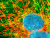
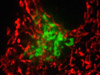
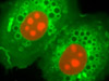
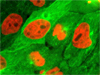
Image Galleries
Featured Article
 Electron Multiplying Charge-Coupled Devices (EMCCDs)
By incorporating on-chip multiplication gain, the electron multiplying CCD achieves, in an all solid-state sensor, the single-photon detection sensitivity typical of intensified or electron-bombarded CCDs at much lower cost and without compromising the quantum efficiency and resolution characteristics of the conventional CCD structure.
Product Information

Review Articles
Concepts in Digital Imaging Technology
Three Phase CCD Clocking
Charge transfer through CCD shift registers occurs after integration in order to relocate accumulated charge information to the sense amplifier, which is physically separated from the parallel pixel array. Several clocking schemes, including the three phase technique illustrated in Figure 1, are utilized to transfer charge from the collection gates to the output node.
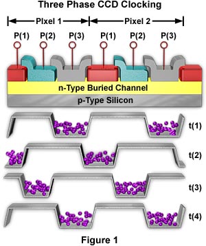
Three phase CCD clocking waveform complement improves spatial resolution over that obtained in four phase devices, yet requires only three gates per pixel. This scheme differs from four phase clocking by using only one storage gate and two barrier gates, which allows for faster frame rates and the fabrication of higher density and resolution CCDs. Another advantage of the technique is the formation of three independent polysilicon layers, one for each set of gate electrodes, so that clock phases are not forced to operate on two gates embedded in the same polysilicon layer. This innovation increases device fabrication yield.
A three phase CCD incorporates three individual polysilicon gate electrodes in each pixel cell, each of which requires a separate input clock signal to properly transport accumulated charge in a scheme that requires a more complex clocking arrangement than that described for the four phase CCD. The shift register illustrated in Figure 1 includes two complete pixel elements, for a total of six gates aligned along a common axis to form a column. The nature of electrostatic forces in the silicon substrate beneath the gates is determined by the voltage level applied to a particular gate by the clock input signal. High level voltages induce the formation of a potential "well" beneath the gate, whereas low level voltages form a potential barrier to electron movement.
The initial state at t(1) of the CCD illustrated in Figure 1 is gates P(1) and P(2) of both Pixels 1 and 2 having low-level voltages (forming potential barriers) and gates P(3) of the pixels with high-level voltages, forming potential wells filled with purple spheres that represent integrated charge (electrons). At t(2), gates P(1) at both pixels are brought to a high voltage, followed shortly, but not simultaneously, by gates P(3) assuming low voltages. The integrated charge now resides under gates P(1) of both pixels. In a similar manner, the charge can be further shifted at t(3) by changing the voltage applied to gates P (1) and P(2), to complete the cycle. At the start of the next cycle (t(4)), the voltage to gates P(2) shifts from high to low, followed by the voltage to gates P(3) shifting from low to high. The net result is that gates P(3) from both pixels now contain charge originally integrated at the previous pixel.
Contributing Authors
Mortimer Abramowitz - Olympus America, Inc., Two Corporate Center Drive., Melville, New York, 11747.
Michael W. Davidson - National High Magnetic Field Laboratory, 1800 East Paul Dirac Dr., The Florida State University, Tallahassee, Florida, 32310.