
Image Galleries
Featured Article
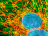
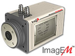 Electron Multiplying Charge-Coupled Devices (EMCCDs)
By incorporating on-chip multiplication gain, the electron multiplying CCD achieves, in an all solid-state sensor, the single-photon detection sensitivity typical of intensified or electron-bombarded CCDs at much lower cost and without compromising the quantum efficiency and resolution characteristics of the conventional CCD structure.
Product Information
Interactive Tutorials
Tools for Digital Imaging Flash Tutorials
Charge-coupled devices (CCDs), like microprocessor and memory integrated circuits, are fabricated on silicon wafers in a series of elaborate steps using photolithography to define and build various functional elements within the microcircuitry. Each wafer contains tens to hundreds of identical devices, each fully capable of producing a single CCD chip for use in digital cameras. This section of the Molecular Expressions Photomicrography Primer contains links to illustrated discussions of important CCD concepts, which are critical in forming a complete understanding of digital imaging techniques.
Avalanche Photodiodes - An avalanche photodiode is a silicon-based semiconductor containing a pn junction consisting of a positively doped p region and a negatively doped n region sandwiching an area of neutral charge termed the depletion region. These diodes provide gain by the generation of electron-hole pairs from an energetic electron that creates an "avalanche" of electrons in the substrate.
Building A Charge-Coupled Device - Explore the steps utilized in the construction of a charge-coupled device (CCD) as a portion of an individual pixel gate is fabricated on a silicon wafer simultaneously with thousands or even millions of neighboring elements. The interactive tutorial examines and illustrates each individual stage in the fabrication of the CCD photodiode sensor element.
CCD Blooming - Under conditions where a CCD is exposed to very high intensity illumination, it is possible to exhaust the storage capacity of the CCD wells, a condition known as blooming. When this occurs, excess charge will overflow into adjacent CCD photodiode wells resulting in a corrupted image near the blooming site. This tutorial explores the operation of a lateral overflow drain to prevent CCD blooming.
CCD Clocking Schemes - Charge transfer through CCD shift registers occurs after integration to relocate accumulated charge information to the sense amplifier, which is physically separated from the parallel pixel array. This tutorial explores several clocking schemes that are utilized to transfer charge from the collection gates to the output node.
CCD Operation - Explore the operation of a charge-coupled device (CCD) imaging semiconductor with this interactive Flash tutorial. Modern CCDs consist of a light-sensitive sandwich of insulating silicon dioxide positioned beneath an array of photodiodes and above an array of metal electrodes.
Pixel Binning - Explore how clock signals controlling a CCD can be used to combine integrated charge from adjacent pixels to improve signal-to-noise ratios and increase the readout frame rate. Instructions for operation of the tutorial appear below the applet window.
Channel Photomultipliers - Channel photomultipliers represent a new head-on monolithic design that incorporates a unique detector having a semitransparent photocathode deposited onto the inner surface of the entrance window. The photomultiplier features similar functionality to conventional units, but with dramatically increased sensitivity and high quantum efficiency. Individual photoelectrons released by the photocathode enter a narrow and curved semiconductive channel that serves in place of the traditional dynode chain. Each time an electron impacts an inner wall of the channel, multiple secondary electrons are emitted. This interactive tutorial explores how electrons are multiplied within the conductive chain of a channel photomultiplier.
Digital Image Sampling Frequency - In order to match the optical and electronic resolution of a microscope and the accompanying camera system, a digital image should have a sufficient number of samples per horizontal line so that the display faithfully represents the original signal presented to the digitizing device. This interactive tutorial explores how variations in specimen sampling frequency affect the resolution of the final image.
Electron-Bombarded CCDs - Electron-bombarded charge-coupled devices (CCDs) are a relatively new development in which photons are detected by a photocathode in a manner similar to an image intensifier. Instructions for operation of the tutorial appear beneath the applet window.
CCD Electronic Shutters - Electronic shutters are employed in charge-coupled devices (CCDs) to control integration time (exposure) of the photodiode array and reduce smear when capturing moving objects in the microscope. Instructions for operation of the tutorial appear beneath the applet window.
Frame-Transfer CCD Operation - Frame-Transfer charged coupled image sensors have an architecture similar to that of full-frame CCDs. These devices have a parallel register that is divided into two separate and identical areas, termed the Image and Storage arrays. Instructions for operation of the tutorial appear below the applet window.
Full-Frame CCD Operation - Full-frame charge-coupled devices (CCDs) feature high-density pixel arrays capable of producing digital images with the highest resolution currently available. This popular CCD architecture has been widely adopted due to the simple design, reliability, and ease of fabrication. Instructions for operation of the tutorial appear beneath the applet window.
Interline CCD Operation - Interline charge-coupled device architecture is designed to compensate for many of the shortcomings of frame-transfer CCDs. These devices are composed of a hybrid structure incorporating a separate photodiode and a CCD storage region, protected with a mask structure, into each pixel element. Instructions for operation of the tutorial appear below the applet window.
Microlens Arrays - Microlens arrays (also referred to as microlenticular arrays or lenslet arrays) are used to increase the optical fill factor in some CCDs, which suffer from reduced aperture due to metal shielding. These tiny lens systems serve to focus and concentrate light onto the photodiode surface instead of allowing it to fall on non-photosensitive areas of the device.
Photomultiplier Tubes - A photomultiplier tube, useful for light detection of very weak signals, is a photoemissive device in which the absorption of a photon results in the emission of an electron. These detectors work by amplifying the electrons generated by a photocathode exposed to a photon flux. Instructions for operating the interactive tutorial appear below the applet window.
Proximity-Focused Image Intensifiers - Image intensifiers were developed for military use to enhance our night vision and are often referred to as wafer tubes or proximity-focused intensifiers. They have a flat photocathode separated by a small gap on the input side of a micro-channel plate (MCP) electron multiplier and a phosphorescent output screen on the reverse side of the MCP.
Side-On Photomultipliers - In the side-on photomultiplier tube design, photons impact an internal photocathode and eject electrons from the front face. These ejected photoelectrons have trajectories angled at the first dynode, which in turn emits a larger quantity of electrons angled at the second dynode (and so on). Instructions for operation of the tutorial appear beneath the applet window.